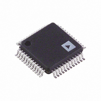
ADG726BSUZ Analog Devices Inc, ADG726BSUZ Datasheet - Page 8

ADG726BSUZ
Manufacturer Part Number
ADG726BSUZ
Description
IC MULTIPLEXER DUAL 16X1 48TQFP
Manufacturer
Analog Devices Inc
Datasheet
1.ADG732BSUZ.pdf
(12 pages)
Specifications of ADG726BSUZ
Function
Multiplexer
Circuit
2 x 16:1
On-state Resistance
5.5 Ohm
Voltage Supply Source
Single, Dual Supply
Voltage - Supply, Single/dual (±)
1.8 V ~ 5.5 V, ±2.5 V
Current - Supply
10µA
Operating Temperature
-40°C ~ 85°C
Mounting Type
Surface Mount
Package / Case
48-TQFP, 48-VQFP
No. Of Circuits
2
Supply Current
10µA
On State Resistance Max
4ohm
Supply Voltage Range
1.8V To 5.5V
Operating Temperature Range
-40°C To +85°C
Analog Switch Case Style
TQFP
Lead Free Status / RoHS Status
Lead free / RoHS Compliant
Available stocks
Company
Part Number
Manufacturer
Quantity
Price
Company:
Part Number:
ADG726BSUZ
Manufacturer:
Analog Devices Inc
Quantity:
1 818
Company:
Part Number:
ADG726BSUZ
Manufacturer:
Analog Devices Inc
Quantity:
10 000
Part Number:
ADG726BSUZ
Manufacturer:
ADI/亚德诺
Quantity:
20 000
Company:
Part Number:
ADG726BSUZ-REEL
Manufacturer:
Analog Devices Inc
Quantity:
10 000
ADG726/ADG732
V
V
I
I
GND
S
D
IN
V
R
∆R
R
I
I
I
V
V
I
C
C
C
C
t
t
t
t
Charge
Injection
OFF Isolation
Crosstalk
ON Response
Insertion
Loss
DD
SS
S
D
D
INL
TRANSITION
ON
OFF
OPEN
DD
SS
D
ON
FLAT(ON)
INL
INH
S
D
D
IN
, I
(OFF)
(OFF)
ON
, C
(OFF)
(V
(EN)
(OFF)
(I
(EN)
S
INH
S
(ON)
S
)
(ON)
)
Most Positive Power Supply Potential
Most Negative Power Supply in a Dual-Supply Application. In single-supply applications, connect to GND.
Positive Supply Current
Negative Supply Current
Ground (0 V) Reference
Source Terminal. May be an input or output.
Drain Terminal. May be an input or output.
Logic Control Input
Analog Voltage on Terminals D and S
Ohmic Resistance between D and S
On Resistance Match between any two channels, i.e., R
Flatness is defined as the difference between the maximum and minimum value of on resistance as measured
over the specified analog signal range.
Source Leakage Current with the Switch OFF
Drain Leakage Current with the Switch OFF
Channel Leakage Current with the Switch ON
Maximum Input Voltage for Logic “0”
Minimum Input Voltage for Logic “1”
Input Current of the Digital Input
OFF Switch Source Capacitance. Measured with reference to ground.
OFF Switch Drain Capacitance. Measured with reference to ground.
ON Switch Capacitance. Measured with reference to ground.
Digital Input Capacitance
Delay Time Measured between the 50% and 90% Points of the Digital Inputs and the Switch ON Condition
when Switching from One Address State to Another
Delay Time between the 50% and 90% Points of the EN Digital Input and the Switch ON Condition
Delay Time between the 50% and 90% Points of the EN Digital Input and the Switch OFF Condition
OFF Time Measured between the 80% Points of Both Switches when Switching from One Address State to Another
A Measure of the Glitch Impulse Transferred from the Digital Input to the Analog Output During Switching
A Measure of Unwanted Signal Coupling through an OFF Switch
A Measure of Unwanted Signal Coupling from One Channel to Another as a Result of Parasitic Capacitance
The Frequency Response of the ON Switch
The Loss Due to the On Resistance of the Switch
TERMINOLOGY
–8–
ON
max – R
ON
min
REV. 0


