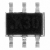
STG3157CTR STMicroelectronics, STG3157CTR Datasheet

STG3157CTR
Specifications of STG3157CTR
Available stocks
Related parts for STG3157CTR
STG3157CTR Summary of contents
Page 1
... V. The IN input is provided to CC control the SPDT switch, and is compatible with standard CMOS output. Switch Table 1. Device summary Order code STG3157CTR April 2010 Low voltage low on-resistance SPDT switch with break-before-make feature = 4 3 2.3 V (connected to common port D) when the IN input = 4 ...
Page 2
Contents Contents 1 Pin connections and functions . . . . . . . . . . . . . . . . . . . . . . . . . . . . . . . . 3 ...
Page 3
STG3157 1 Pin connections and functions Figure 1. Pin connections and IEC logic symbols Table 2. Truth table High impedance Table 3. Pin descriptions Pin Nº Figure 2. Input equivalent ...
Page 4
... These are stress ratings only and operation of the device at these or any other conditions above those indicated in the operating sections of this specification is not implied. Exposure to absolute maximum rating conditions for extended periods may affect device reliability. Refer also to the STMicroelectronics SURE Program and other relevant quality documents. Table 4. ...
Page 5
STG3157 3 Electrical characteristics 3.1 DC Electrical characteristics Table 6. DC specifications Test conditions Symbol Parameter Vcc (V) 1.65-1.95 High level V input 2.3-2.5 IH voltage 2.7-3.6 1.65-1.95 Low level V input 2.3-2.5 IL voltage 2.7-3.6 4.5 3.0 Switch on- ...
Page 6
Electrical characteristics Table 6. DC specifications (continued) Test conditions Symbol Parameter Vcc (V) 5.0 3.3 On- R resistance FLAT flatness 2.5 1.8 OFF state I leakage 1.65-195 OFF current Input I leakage 0 - 5.5 IN current Quiescent I supply ...
Page 7
STG3157 3.2 AC Electrical characteristics = 500 Ω pF Table 7. AC specification Symbol Parameter Vcc (V) 1.65-1.95 2.3-2.7 Propagation delay 3.0-3.3 4.5-5.5 1.65-1.95 2.3-2.7 Output enable t , ...
Page 8
Electrical characteristics 3.3 Analog switch characteristics = 50 Ω pF Table 8. Analog switch characteristics Test conditions Symbol Parameter Vcc (V) OIRR Off isolation 1.65-5.5 Xtalk Crosstalk 1.65-5.5 -3dB BW 1.65-5.5 bandwidth Control ...
Page 9
STG3157 4 Test circuits Figure 3. On-resistance Figure 5. OFF leakage Figure 7. OFF isolation Figure 4. Bandwidth Figure 6. Channel-to-channel crosstalk Figure 8. ON leakage Doc ID 9007 Rev 2 Test circuits 9/18 ...
Page 10
Test circuits Figure 9. Test circuit Table 9. Test circuit Note 5/ equivalent: (includes jig capacitance Ω or equivalent pulse generator (typically 50 Ω OUT Figure ...
Page 11
STG3157 Figure 11. Switching time and charge injection Figure 12. Charge injection ( Ω MΩ, C GEN GEN L Doc ID 9007 Rev 2 Test circuits = 100 pF) L 11/18 ...
Page 12
Package information 5 Package information In order to meet environmental requirements, ST offers these devices in different grades of ® ECOPACK packages, depending on their level of environmental compliance. ECOPACK specifications, grade definitions and product status are available at: www.st.com. ...
Page 13
STG3157 Table 10. SOT323-6L Dim Figure 13. Package dimensions mechanical data mm. Min. Typ. Max. 0.80 1.10 0.00 0.10 0.80 1.00 0.15 0.30 0.10 0.18 1.80 2.20 1.80 2.40 ...
Page 14
Package information Table 11. SOT323-6L footprint recommendation Dim Figure 14. SOT323-6L footprint recommendation 14/18 mm. 2.88 0.78 0.36 0.65 1.05 1.65 Doc ID 9007 Rev 2 STG3157 inch 0.113 0.031 0.014 0.026 0.041 0.065 ...
Page 15
STG3157 Table 12. SOT323-6L tape information Dim max. D1 min max Ao, Bo, Ko Figure 15. SOT323-6L tape information mm. 1.50 +0.1/0 1.75 ±0.1 4.00 ±0.1 0.40 1 3.5 ±0.05 ...
Page 16
Package information Table 13. SOT323-6L reel information Dim Tape size A max. B min min. N min max. Figure 16. SOT323-6L reel information 16/18 mm. 8.0 ±0.30 180.0 1.5 13.0 ±0.20 20.2 60 8.4 +2/-0 14.4 ...
Page 17
STG3157 6 Revision history Table 14. Document revision history Date 02-Sep-2002 19-Apr-2010 Revision 1 Initial release. Document reformatted. In the Features list on the coverpage, updated the “Latch-up performance exceeds” value from 300 mA to 150 mA. Minor text changes ...
Page 18
... Information in this document is provided solely in connection with ST products. STMicroelectronics NV and its subsidiaries (“ST”) reserve the right to make changes, corrections, modifications or improvements, to this document, and the products and services described herein at any time, without notice. All ST products are sold pursuant to ST’s terms and conditions of sale. ...


