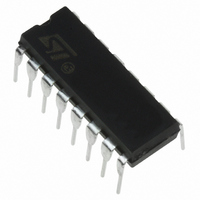
HCF4051BEY STMicroelectronics, HCF4051BEY Datasheet - Page 2

HCF4051BEY
Manufacturer Part Number
HCF4051BEY
Description
IC MUX/DEMUX 8X1 16DIP
Manufacturer
STMicroelectronics
Series
4000Br
Type
Analog Multiplexerr
Specifications of HCF4051BEY
Function
Multiplexer/Demultiplexer
Circuit
1 x 8:1
On-state Resistance
280 Ohm
Voltage Supply Source
Dual Supply
Voltage - Supply, Single/dual (±)
±3 V ~ 20 V
Current - Supply
.08µA
Operating Temperature
-55°C ~ 125°C
Mounting Type
Through Hole
Package / Case
16-DIP (0.300", 7.62mm)
Number Of Channels
1 Channel
On Resistance (max)
1050 Ohms
Propagation Delay Time
60 ns
On Time (max)
720 ns
Off Time (max)
450 ns
Supply Voltage (max)
20 V
Supply Voltage (min)
3 V
Maximum Power Dissipation
200 mW
Maximum Operating Temperature
+ 125 C
Minimum Operating Temperature
- 55 C
Mounting Style
Through Hole
Number Of Switches
Single
Capacitance, Input
5 pF (Typ.) @ 25 °C
Circuit Type
Monolithic Integrated
Current, Input
± 10 mA
Current, Input, Leakage
± 1 μA (Max.)
Current, Supply
3000 μA
Function Type
8-Channels
Logic Function
Multiplexer/Demultiplexer
Logic Type
MOS
Number Of Circuits
Single
Package Type
DIP-16
Power Dissipation
500 mW @ 65 °C
Temperature, Operating, Maximum
125 °C
Temperature, Operating, Minimum
-55 °C
Temperature, Operating, Range
-55 to +125 °C
Time, Delay, Propagation
30 ns (Typ.)
Voltage, Supply
3 to 20 V
Low In.onin. Resistance
125W (Typ.) over 15V p.p signal-input range for VDD - VEE == 15V
High In.offin. Resistance
channel leakage +⁄- 100pA (Typ.) at VDD - VEE == 18V
High Degree Of Linearity
0.5%
Package
16PDIP
Maximum On Resistance
1050@5V Ohm
Maximum Propagation Delay Bus To Bus
20@15V|30@10V|60@5V ns
Multiplexer Architecture
8:1
Maximum Turn-off Time
450@5V ns
Maximum Turn-on Time
720@5V ns
Power Supply Type
Single
Lead Free Status / RoHS Status
Lead free / RoHS Compliant
Other names
497-1361-5
Available stocks
Company
Part Number
Manufacturer
Quantity
Price
ABSOLUTE MAXIMUM RATINGS
Absolute Maximum Ratings are those values beyond which damage to the device may occur. Functional operation under these conditions is
not implied.
All voltage values are referred to V
(*) 500mW at 65 C; derate to 300mW by 10mW/ C from 65 C to 85 C
RECOMMENDED OPERATING CONDITIONS
Symbol
Symbol
V
V
T
T
T
P
V
V
stg
DD
I
DD
op
op
I
D
I
I
Supply Voltage
DC Input Voltage
DC Input Current
Power Dissipation per Package
Power Dissipation per Output Transistor
Operating Temperature
Storage Temperature
Supply Voltage
Input Voltage
Operating Temperature
SS
pin voltage.
Parameter
Parameter
-0.5 to V
-55 to +125
-65 to +150
-0.5 to +22
-55 to 125
0 to V
500 (*)
3 to 20
Value
Value
100
10
DD
DD
+ 0.5
HCF4051B
Unit
Unit
mW
mW
mA
°C
°C
°C
V
V
V
V
3/10


