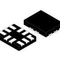
STG3220QTR STMicroelectronics, STG3220QTR Datasheet

STG3220QTR
Specifications of STG3220QTR
Available stocks
Related parts for STG3220QTR
STG3220QTR Summary of contents
Page 1
... ESD performance exceeds JESD22: – Dn pins: 4000-V human body model (A114-A) – All other pins: 2000-V human body model (A114-A) Applications ■ Mobile phones Table 1. Device summary Order code STG3220QTR May 2009 Low voltage high bandwidth dual SPDT switch = 85 ° Description = 2 3 ...
Page 2
Contents Contents 1 Pin settings . . . . . . . . . . . . . . . . . . . . . . . . . . . . . . . . . . . ...
Page 3
STG3220 1 Pin settings Figure 1. Pin connection (top through view) Table 2. Pin description Pin number Symbol Name and function INT Interrupt VCC Positive supply voltage SEL Control 2S1 ...
Page 4
Logic diagram 2 Logic diagram Figure 2. Logic block diagram Figure 3. Logic equivalent circuit Table 3. Truth table SEL High impedance. 4/23 Switch nS1 ON (1) OFF Doc ID 15647 Rev 1 STG3220 Switch nS2 (1) ...
Page 5
STG3220 3 Dedicated port charging detection The STG3220 has a built-in dedicated port charging detection circuit to detect the condition when the USB D+/D- lines are both in high state. When this occurs, the device sends an interrupt signal to ...
Page 6
Maximum rating 4 Maximum rating Stressing the device above the rating listed in the “Absolute maximum ratings” table may cause permanent damage to the device. These are stress ratings only and operation of the device at these or any other ...
Page 7
STG3220 5 Electrical characteristics Table 6. DC specifications Symbol Parameter 1.65 – 1.95 2.3 – 2.5 High level input 2.7 – 3 voltage 3.3 – 3.6 1.65 – 1.95 2.3 – 2.5 Low level input V 2.7 – ...
Page 8
Electrical characteristics Table 6. DC specifications (continued) Symbol Parameter ON resistance ∆R match between ON (1) channels ON resistance R FLAT (2) flatness OFF state I leakage current OFF (Sn), (D) Input leakage 4.3 IN current Quiescent ...
Page 9
STG3220 Table 7. AC characteristics (C Symbol Parameter 1.65 - 1.95 2.3 - 2.7 Propagation t t PLH, PHL delay 3.0 - 3.3 3.6 - 4.3 1.65 - 1.95 V 2.3 - 2.7 t Turn on time ON 3.0 - ...
Page 10
Electrical characteristics Table 8. AC electrical characteristics (C Symbol Parameter Q Charge injection (1) OIRR OFF isolation 1.65 – 4.3 Xtalk Crosstalk 1.65 – 4.3 BW -3dB bandwidth Control pin input C IN capacitance Sn port capacitance C ON when ...
Page 11
STG3220 Table 9. USB related AC electrical characteristics Symbol Parameter Channel-to- t SK(0) channel skew Skew of opposite t SK(P) transition of the same output T Total jitter J V Test CC T (V) conditions Min 3.0 - 3.6 C ...
Page 12
Test circuit 6 Test circuit Figure 5. ON resistance VS GND 12/ GND Doc ID 15647 Rev 1 STG3220 D CS14071 ...
Page 13
STG3220 Figure 6. OFF leakage V SS Figure 7. OFF isolation S(OFF GND GND GND Doc ID 15647 Rev 1 Test circuit I D(OFF) D ...
Page 14
Test circuit Figure 8. Bandwidth Figure 9. Channel-to-channel crosstalk 14/ GND Doc ID 15647 Rev 1 STG3220 D V OUT CS00371 CS14091 ...
Page 15
STG3220 Figure 10. Test circuit 5/ equivalent (includes jig and probe capacitance Ω or equivalent pulse generator (typically 50 Ω OUT Doc ID ...
Page 16
Test circuit Figure 11. Break-before-make time delay Figure 12. Switching time and charge injection ( GEN GEN Figure 13. Turn ON, turn OFF delay time 16/ Ω MΩ ...
Page 17
STG3220 7 Package mechanical data In order to meet environmental requirements, ST offers these devices in different grades of ® ECOPACK packages, depending on their level of environmental compliance. ECOPACK specifications, grade definitions and product status are available at: www.st.com. ...
Page 18
Package mechanical data Table 2. Mechanical data for QFN10 (1.8 x 1.4 x 0.5 mm) - 0.4 mm pitch Symbol Figure 15. Footprint recommendations for QFN10 (1.8 x 1.4 x 0.5 mm) ...
Page 19
STG3220 Figure 16. Carrier tape for QFN10 (1.8 x 1.4 x 0.5 mm) - 0.4 mm pitch Doc ID 15647 Rev 1 Package mechanical data 19/23 ...
Page 20
Package mechanical data Figure 17. Reel information (front side) for QFN10 (1.8 x 1.4 x 0.5 mm) - 0.4 mm pitch 20/23 Doc ID 15647 Rev 1 STG3220 ...
Page 21
STG3220 Figure 18. Reel information (back view) for QFN10 (1.8 x 1.4 x 0.5 mm) - 0.4 mm pitch Doc ID 15647 Rev 1 Package mechanical data 21/23 ...
Page 22
Revision history 8 Revision history Table 10. Document revision history Date 14-May-2009 22/23 Revision 1 Initial release. Doc ID 15647 Rev 1 STG3220 Changes ...
Page 23
... STG3220 Information in this document is provided solely in connection with ST products. STMicroelectronics NV and its subsidiaries (“ST”) reserve the right to make changes, corrections, modifications or improvements, to this document, and the products and services described herein at any time, without notice. All ST products are sold pursuant to ST’s terms and conditions of sale. ...


