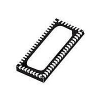
ST3DV520AQTR STMicroelectronics, ST3DV520AQTR Datasheet - Page 6

ST3DV520AQTR
Manufacturer Part Number
ST3DV520AQTR
Description
IC MUX/DEMUX 2X2 56QFN
Manufacturer
STMicroelectronics
Specifications of ST3DV520AQTR
Function
Multiplexer/Demultiplexer
Circuit
5 x 2:2
On-state Resistance
6.5 Ohm
Voltage Supply Source
Single Supply
Voltage - Supply, Single/dual (±)
3 V ~ 3.6 V
Current - Supply
150µA
Operating Temperature
-40°C ~ 85°C
Mounting Type
Surface Mount
Package / Case
56-QFN
Number Of Bits
10 to 20
Propagation Delay Time
0.25 ns
Supply Voltage (max)
3.6 V
Supply Voltage (min)
3 V
Maximum Operating Temperature
+ 85 C
Minimum Operating Temperature
- 40 C
Mounting Style
SMD/SMT
Power Dissipation
500 mW
Lead Free Status / RoHS Status
Lead free / RoHS Compliant
Other names
497-10388-2
Available stocks
Company
Part Number
Manufacturer
Quantity
Price
Company:
Part Number:
ST3DV520AQTR
Manufacturer:
BROADCOM
Quantity:
50
Electrical characteristics
3
Table 6.
1. Refer to
2. Measured by voltage drop between channels at indicated current through the switch. ON resistance is determined by the
3. Flatness is defined as the difference between the R
4.
6/19
IOFF
IOFF
Symbol
lower of the voltages.
Δ
Δ
R
R
R
V
V
V
I
R
I
FLAT
IH
(SW)
ON
IL
ON
IH
IK
IL
(SEL)
ON
measured at same V
(1)
Figure 4: Test circuit for leakage current (IOFF) on page 9
Electrical characteristics
DC electrical characteristics (V
Voltage input high (SEL)
Voltage input low
(SEL)
Clamp diode voltage
(SEL)
Input high current
(SEL)
Input low current
(SEL)
Leakage current through
the switch common
terminals (A to J)
SEL pin leakage current
Switch ON resistance
ON resistance flatness
(3)
ON resistance match
between channel
Δ
(2)(4)
R
ON
= R
Parameter
ONMAX
CC
, temperature and voltage level.
-R
ONMIN
(2)
(2)
High level guaranteed
Low level guaranteed
V
I
V
V
V
V
V
A to J = V
LED1 to LED3 = V
A0 to J0 = 0 V
A1 to J1 = floating
SEL = V
V
SEL = 0 to 3.6 V
V
V
I
V
V
I
V
V
I
IN
IN
IN
IN
CC
CC
IN
CC
IN
CC
CC
CC
IN
CC
IN
CC
IN
= -18 mA
= -40 mA
= -40 mA
= -40 mA
= V
= GND
= 1.5 to V
at 1.5 and VCC
= 1.5 to V
= 3.6 V
= 3.6 V
= 3.6 V
= 3.6 V
= 0 V
= 3.0 V
= 3.0 V
= 3.0 V
Doc ID 16885 Rev 2
Test condition
ONMAX
CC
CC
CC
CC
= 3.3 V ±10%)
and R
CC
CC
CC
ONMIN
of ON resistance over the specified range.
Min
-0.5
2
–
–
–
–
–
–
–
–
-40 to 85 °C
Value
Typ
-0.8
4.0
0.5
0.4
–
–
–
–
–
–
Max
-1.2
0.8
6.5
±5
±5
±1
±1
–
–
1
ST3DV520A
Unit
µA
µA
µA
µA
Ω
Ω
Ω
V
V
V


