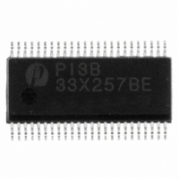
PI3B33X257BE Pericom Semiconductor, PI3B33X257BE Datasheet - Page 3

PI3B33X257BE
Manufacturer Part Number
PI3B33X257BE
Description
IC MUX/DEMUX QUAD 1X2 48BQSOP
Manufacturer
Pericom Semiconductor
Datasheet
1.PI3B33X257BE.pdf
(4 pages)
Specifications of PI3B33X257BE
Function
Multiplexer/Demultiplexer
Circuit
4 x 1:2
On-state Resistance
15 Ohm
Current - Supply
9µA
Operating Temperature
-40°C ~ 85°C
Mounting Type
Surface Mount
Package / Case
48-BQSOP
Configuration
4 x 2:1
Number Of Inputs
24
Number Of Outputs
12
Operating Supply Voltage (typ)
3.3V
Operating Supply Voltage (min)
3.135V
Operating Supply Voltage (max)
3.465V
Power Dissipation
500mW
Operating Temp Range
-40C to 85C
Operating Temperature Classification
Industrial
Mounting
Surface Mount
Pin Count
48
Package Type
BQSOP
Lead Free Status / RoHS Status
Lead free / RoHS Compliant
Available stocks
Company
Part Number
Manufacturer
Quantity
Price
Capacitance
Notes:
1.
2.
3.
4.
Power Supply Characteristics
Notes:
1.
2.
3.
Switching Characteristics over Operating Range
Notes:
1.
2.
3.
C
C
C
I
ΔI
t
t
t
t
t
t
Parameters
IY
SY
PZH
PZL
PHZ
PLZ
CC
Parameters
IN
OFF
ON
CC
Parameters
For Max. or Min. conditions, use appropriate value specified under Electrical Characteristics for the applicable device type.
Typical values are at V
Measured by the voltage drop between I and Y pin at indicated current through the switch. ON resistance is determined by the lower of the
voltages on the two (I,Y) pins.
This parameter is determined by device characterization but is not production tested.
For Max. or Min. conditions, use appropriate value specified under Electrical Characteristics for the applicable device.
Typical values are at V
Per TTL driven input (V
See test circuit and waveforms.
This parameter is guaranteed but not tested on Propagation Delays.
The bus switch contributes no propagational delay other than the RC delay of the ON resistance of the switch and the load capacitance. The
time constant for the switch alone is of the order of 0.25ns for 50pF load. Since this time constant is much smaller than the rise/fall times of
typical driving signals, it adds very little propagational delay to the system. Propagational delay of the bus switch when used in a system is
determined by the driving circuit on the driving side of the switch and its interaction with the load on the driven side.
Propagation Delay
In to Yn
Bus Select Time
Sn to Yn
Bus Disable Time
E to Yn
Bus Disable Time
E to Yn
(T
(4)
Quiescent Power
Supply Current
Supply Current per
Input @ TTL HIGH
A
= 25°C, f = 1 MHz)
Input Capacitance
In/Yn Capacitance, Switch Off
In/Yn Capacitance, Switch On
Description
CC
CC
IN
= 3.3V, T
= 3.3V, +25°C ambient.
= 3.4V, control inputs only); I and Y pins do not contribute to I
Description
(2,3)
A
= 25°C ambient and maximum loading.
Description
V
V
CC
CC
= Max.
= Max.
Test Conditions
Test Conditions
V
V
3
R
C
IN
IN
L
L
= GND or V
= 3.0V
= 500Ω
= 50pF
Test Conditions
(1)
V
(3)
IN
(1)
= 0V
CC
3.3V, 24:12 Mux/DeMux NanoSwitch
CC
.
Min.
Min.
1
1
1
Typ.
17.0
25.0
3.0
Typ.
Com.
0.1
(2)
Max.
0.25
Max.
4.5
4.5
4.8
Max.
PS8334D
750
9.0
PI3B33X257
Units
Units
pF
Units
ns
µA
11/01/04
™


