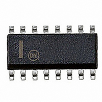
MC74LVX4053DG ON Semiconductor, MC74LVX4053DG Datasheet

MC74LVX4053DG
Specifications of MC74LVX4053DG
Available stocks
Related parts for MC74LVX4053DG
MC74LVX4053DG Summary of contents
Page 1
MC74LVX4053 Analog Multiplexer/ Demultiplexer High−Performance Silicon−Gate CMOS The MC74LVX4053 utilizes silicon−gate CMOS technology to achieve fast propagation delays, low ON resistances, and low OFF leakage currents. This analog multiplexer/demultiplexer controls analog voltages that may vary across the complete power supply ...
Page 2
... NONE Don’t Care ORDERING INFORMATION Device MC74LVX4053D MC74LVX4053DG MC74LVX4053DR2 MC74LVX4053DR2G MC74LVX4053DT MC74LVX4053DTG MC74LVX4053DTR2 MC74LVX4053DTR2G MC74LVX4053M MC74LVX4053MG MC74LVX4053MEL MC74LVX4053MELG †For information on tape and reel specifications, including part orientation and tape sizes, please refer to our Tape and Reel Packaging Specifications Brochure, BRD8011/D. ...
Page 3
MAXIMUM RATINGS Î Î Î Î Î ...
Page 4
DC CHARACTERISTICS − Digital Section Symbol Parameter V Minimum High−Level Input IH Voltage, Channel−Select or En- able Inputs V Maximum Low−Level Input IL Voltage, Channel−Select or En- able Inputs I Maximum Input Leakage IN Current, Channel−Select or En- able Inputs ...
Page 5
AC CHARACTERISTICS ( pF, Input t L Symbol Parameter t , Maximum Propagation Delay, PLH t Channel−Select to Analog Output PHL (Figures 16 and 17 Maximum Propagation Delay, Enable to PLZ t Analog Output (Figures 14 ...
Page 6
PROGRAMMABLE POWER SUPPLY OFF OFF Figure 5. Maximum Off Channel Leakage Current, Any One Channel, Test Set−Up HP4195A Network Anl HP11667B ...
Page 7
HP4195A Network Anl 0 HP11667B V IS Pwr Splitter 100 KW 0.1 mF All untested Analog I/O pins Config = Network Format = T/R (dB) CAL = Trans Cal ...
Page 8
ON/OFF OFF/ON Enable − *Includes all probe and jig capacitance OUT OUT Figure 10. Charge Injection, Test Set−Up HP4195A Network ...
Page 9
Tek 11801B DSO COM INPUT OFF − Figure 12. Break−Before−Make, Test Set−Up CHANNEL 50% SELECT t PLH ANALOG 50% OUT Figure 14. Propagation Delays, Channel ...
Page 10
ON/OFF OFF/ − 11 − 14 Channel Select Figure 18. Power Dissipation Capacitance, Test Set−Up HP3466 )V DMM COM HP3466 )V DMM COM HP E3630A DC Pwr Supply COM ...
Page 11
The Channel Select and Enable control pins should GND logic levels. V being recognized as a logic CC CC high and GND being recognized as a logic low. In this example ...
Page 12
LEVEL A SHIFTER 10 LEVEL B SHIFTER 9 LEVEL C SHIFTER 6 LEVEL ENABLE SHIFTER Figure 23. Function Diagram, LVX4053 http://onsemi.com ...
Page 13
... G K −T− SEATING PLANE 0.25 (0.010 *For additional information on our Pb−Free strategy and soldering details, please download the ON Semiconductor Soldering and Mounting Techniques Reference Manual, SOLDERRM/D. PACKAGE DIMENSIONS SOIC−16 D SUFFIX CASE 751B−05 ISSUE K −B− 0.25 (0.010 ...
Page 14
... −V− C 0.10 (0.004) −T− SEATING D PLANE 16X 0.36 *For additional information on our Pb−Free strategy and soldering details, please download the ON Semiconductor Soldering and Mounting Techniques Reference Manual, SOLDERRM/D. PACKAGE DIMENSIONS TSSOP−16 DT SUFFIX CASE 948F−01 ISSUE Ç ...
Page 15
... Opportunity/Affirmative Action Employer. This literature is subject to all applicable copyright laws and is not for resale in any manner. PUBLICATION ORDERING INFORMATION LITERATURE FULFILLMENT: Literature Distribution Center for ON Semiconductor P.O. Box 5163, Denver, Colorado 80217 USA Phone: 303−675−2175 or 800−344−3860 Toll Free USA/Canada Fax: 303− ...


