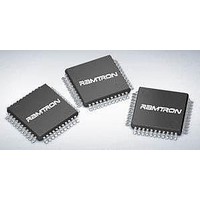
VRS51C1000-40-QG Ramtron, VRS51C1000-40-QG Datasheet - Page 33

VRS51C1000-40-QG
Manufacturer Part Number
VRS51C1000-40-QG
Description
Microcontrollers (MCU) 64K+1K 40MHz 5V
Manufacturer
Ramtron
Datasheet
1.VRS51C1000-40-PG.pdf
(48 pages)
Specifications of VRS51C1000-40-QG
Data Bus Width
8 bit
Program Memory Type
Flash
Program Memory Size
64 KB
Data Ram Size
1 KB
Interface Type
UART
Maximum Clock Frequency
40 MHz
Number Of Programmable I/os
36
Number Of Timers
3
Operating Supply Voltage
4.5 V to 5.5 V
Maximum Operating Temperature
+ 85 C
Mounting Style
SMD/SMT
Package / Case
QFP-44
Minimum Operating Temperature
- 40 C
Data Rom Size
128 B
Height
2 mm
Length
10 mm
Supply Voltage (max)
5.5 V
Supply Voltage (min)
4.5 V
Width
10 mm
Lead Free Status / Rohs Status
Details
PWM Registers - Port1 Configuration Register
T
PWM Registers -PWM Control Register
The following table describes the PWM Control
Register.
T
The following table describes the relationship between
the values of PDCK1/PDCK0 and the value of the
divider. Numerical values of the corresponding
frequencies are also provided.
______________________________________________________________________________________________
www.ramtron.com
ABLE
ABLE
[2:0]
[7:2]
PDCK1
Bit
Bit
VRS51C1000
7
6
5
4
3
1
0
7
PWM4E
PWM0E
0
0
1
1
39: P
40: PWM C
7
3
ORT
Mnemonic
Mnemonic
PWM4E
PWM3E
PWM2E
PWM1E
PWM0E
Unused
Unused
6
PDCK1
PDCK0
PDCKO
1 C
ONTROL
ONFIGURATION
0
1
0
1
5
Unused
R
PWM3E
EGISTER
Divider
Description
-
Input Clock Frequency Divider Bit 1
Input Clock Frequency Divider Bit 0
Description
When bit is set to one, the
corresponding PWM pin is active as
a PWM function. When the bit is
cleared, the corresponding PWM pin
is active as an I/O pin. These five
bits are cleared upon reset.
-
6
2
R
16
2
4
8
EGISTER
4
(PWMC) – SFR A3
(PWME, $9B)
3
Fosc=20MHz
PWM clock,
1.25MHz
PWM2E
2.5MHz
Unused
10MHz
5MHz
5
1
H
2
PDCK1
1
Fosc=24MHz
PWM clock,
PWM1E
1.5MHz
12MHz
6MHz
3MHz
4
0
PDCK0
0
PWM Data Registers
The
Registers. The PWMDx bits hold the content of the
PWM Data Register and determine the duty cycle of
the PWM output waveforms. The NP[2:0] bits will insert
narrow pulses into the 8-PWM-cycle frame.
T
T
T
ABLE
ABLE
ABLE
PWMD0.0
Bit
7
6
5
4
3
2
1
0
Bit
7
6
5
4
3
2
1
0
Bit
7
6
5
4
3
2
1
0
PWMD0.4
PWMD1.4
PWMD1.0
PWMD2.4
PWMD2.0
41: PWM D
42: PWM D
43: PWM D
Mnemonic
PWMD0.4
PWMD0.3
PWMD0.2
PWMD0.1
PWMD0.0
NP0.2
NP0.1
NP0.0
Mnemonic
PWMD1.4
PWMD1.3
PWMD1.2
PWMD1.1
PWMD1.0
NP1.2
NP1.1
NP1.0
Mnemonic
PWMD2.4
PWMD2.3
PWMD2.2
PWMD2.1
PWMD2.0
NP2.2
NP2.1
NP2.0
following
7
3
7
3
7
3
ATA
ATA
ATA
R
R
R
EGISTER
EGISTER
EGISTER
PWMD0.3
PWMD1.3
PWMD2.3
tables
NP0.2
NP1.2
NP2.2
Description
Contents of PWM Data Register 0 Bit 4
Contents of PWM Data Register 0 Bit 3
Contents of PWM Data Register 0 Bit 2
Contents of PWM Data Register 0 Bit 1
Contents of PWM Data Register 0 Bit 0
Inserts Narrow Pulses in a 8-PWM-Cycle
Frame
Description
Contents of PWM Data Register 1 Bit 4
Contents of PWM Data Register 1 Bit 3
Contents of PWM Data Register 1 Bit 2
Contents of PWM Data Register 1 Bit 1
Contents of PWM Data Register 1 Bit 0
Inserts Narrow Pulses in a 8-PWM-Cycle
Frame
Description
Contents of PWM Data Register 2 Bit 4
Contents of PWM Data Register 2 Bit 3
Contents of PWM Data Register 2 Bit 2
Contents of PWM Data Register 2 Bit 1
Contents of PWM Data Register 2 Bit 0
Inserts Narrow Pulses in a 8-PWM-Cycle
Frame
6
2
6
2
6
2
0 (PWMD0) – SFR A4
1 (PWMD1) – SFR A5
2 (PWMD2) – SFR A6
describe
PWMD0.2
PWMD1.2
PWMD2.2
NP0.1
NP1.1
NP2.1
page 33 of 48
5
1
5
1
5
1
H
H
H
the
PWM
PWMD0.1
PWMD1.1
PWMD2.1
NP0.0
NP1.0
NP2.0
4
0
4
0
4
0
Data


