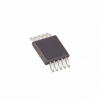
MAX4736EUB+ Maxim Integrated Products, MAX4736EUB+ Datasheet - Page 7

MAX4736EUB+
Manufacturer Part Number
MAX4736EUB+
Description
IC SWITCH DUAL SPDT 10UMAX
Manufacturer
Maxim Integrated Products
Datasheet
1.MAX4736EUB.pdf
(14 pages)
Specifications of MAX4736EUB+
Function
Switch
Circuit
2 x SPDT
On-state Resistance
800 mOhm
Voltage Supply Source
Single Supply
Voltage - Supply, Single/dual (±)
1.6 V ~ 4.2 V
Current - Supply
1µA
Operating Temperature
-40°C ~ 85°C
Mounting Type
Surface Mount
Package / Case
10-MSOP, Micro10™, 10-uMAX, 10-uSOP
Number Of Switches
Dual
Switch Configuration
SPDT
On Resistance (max)
1 Ohms
On Time (max)
30 ns
Off Time (max)
25 ns
Off Isolation (typ)
- 52 dB
Bandwidth
130 MHz
Supply Voltage (max)
3.6 V
Supply Voltage (min)
1.6 V
Supply Current
1 uA
Maximum Power Dissipation
444 mW
Maximum Operating Temperature
+ 55 C
Mounting Style
SMD/SMT
Minimum Operating Temperature
- 40 C
Off State Leakage Current (max)
5 nA
Lead Free Status / RoHS Status
Lead free / RoHS Compliant
The MAX4736 is a low 0.8Ω max (at V+ = 2.7V) on-
resistance, low-voltage, dual SPDT analog switch that
operates from a 1.6V to 4.2V single supply. CMOS
switch construction allows switching analog signals that
range from GND to V+.
When powered from a 2.7V supply, the 0.8Ω max R
allows high continuous currents to be switched in a
variety of applications.
Proper power-supply sequencing is recommended for
all CMOS devices. Do not exceed the absolute maxi-
mum ratings; stresses beyond the listed ratings can
cause permanent damage to the devices. Always
sequence V+ on first, followed by NO_, NC_, or COM_.
Although it is not required, power-supply bypassing
improves noise margin and prevents switching noise
propagation from the V+ supply to other components.
A 0.1µF capacitor, connected from V+ to GND, is ade-
quate for most applications.
Figure 1. Switching Time
MAX4736
0.6Ω, Low-Voltage, Single-Supply, Dual SPDT
LOGIC
INPUT
V
IN
Applications Information
_______________________________________________________________________________________
C
L
NC_ or NO_
NO_ or NC_
IN_
INCLUDES FIXTURE AND STRAY CAPACITANCE.
Detailed Description
GND
V+
V+
COM_
R
L
V
OUT
C
ON
L
The MAX4736 logic inputs can be driven up to 3.6V,
regardless of the supply voltage. For example, with a 1.8V
supply, IN_ can be driven low to GND and high to 3.6V.
Driving IN_ rail-to-rail minimizes power consumption.
Analog signals that range over the entire supply voltage
(V+ to GND) can be passed with very little change in on-
resistance (see Typical Operating Characteristics). The
switches are bidirectional, so the NO_, NC_, and COM_
pins can be used as either inputs or outputs.
High-speed switches require proper layout and design
procedures for optimum performance. Reduce stray
inductance and capacitance by keeping traces short
and wide. Ensure that bypass capacitors are as close
to the device as possible. Use large ground planes
where possible.
SWITCH
OUTPUT
LOGIC
INPUT
V
IN_
Test Circuits/Timing Diagrams
= V
IH
0
0
+ 0.5V
LOGIC INPUT WAVEFORMS INVERTED FOR SWITCHES
THAT HAVE THE OPPOSITE LOGIC SENSE.
V
t
Analog Switch
50%
ON
OUT
0.9
✕
Analog Signal Levels
V
0UT
t
OFF
t r < 5ns
t f < 5ns
0.9
Logic Inputs
✕
V
OUT
Layout
7


