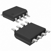
DG418DY+ Maxim Integrated Products, DG418DY+ Datasheet - Page 4

DG418DY+
Manufacturer Part Number
DG418DY+
Description
IC SWITCH SPST 8SOIC
Manufacturer
Maxim Integrated Products
Type
Analog Switchr
Datasheet
1.DG418DY.pdf
(12 pages)
Specifications of DG418DY+
Function
Switch
Circuit
1 x SPST- NO
On-state Resistance
35 Ohm
Voltage Supply Source
Single, Dual Supply
Voltage - Supply, Single/dual (±)
10 V ~ 30 V, ±4.5 V ~ 20 V
Operating Temperature
-40°C ~ 85°C
Mounting Type
Surface Mount
Package / Case
8-SOIC (0.154", 3.90mm Width)
Number Of Switches
Dual
Switch Configuration
SPST
On Resistance (max)
35 Ohms
On Time (max)
175 ns
Off Time (max)
145 ns
Off Isolation (typ)
68 dB
Supply Voltage (max)
+/- 20 V
Supply Voltage (min)
+/- 4.5 V
Supply Current
- 0.0001 uA
Maximum Power Dissipation
471 mW
Maximum Operating Temperature
+ 85 C
Mounting Style
SMD/SMT
Description/function
Analog Switch
Input Level
CMOS, TTL
Minimum Operating Temperature
- 40 C
Off State Leakage Current (max)
5 nA
Package
8SOIC N
Maximum On Resistance
100@10.8V Ohm
Maximum High Level Output Current
30 mA
Maximum Turn-off Time
145@±15V ns
Maximum Turn-on Time
175@±15V ns
Switch Architecture
SPST
Power Supply Type
Single|Dual
Lead Free Status / RoHS Status
Lead free / RoHS Compliant
ELECTRICAL CHARACTERISTICS—Single Supply
(V+ = +12V, V- = 0V, VL = 5V, GND = 0V, V
Improved, SPST/SPDT Analog Switches
Note 2: Typical values are for design aid only, are not guaranteed, and are not subject to production testing. The algebraic
Note 3: Guaranteed by design.
Note 4: On-resistance match between channels and flatness is guaranteed only with bipolar-supply operation. Flatness is defined as
Note 5: Leakage parameters I
Note 6: Off-Isolation Rejection Ratio = 20log (V
Note 7: Between any two switches.
4
SWITCH
DYNAMIC
SUPPLY
Analog Signal Range
Drain-Source On-Resistance
Turn-On Time
Turn-Off Time
Break-Before-Make Interval
Charge Injection (Note 3)
Positive Supply Current
Negative Supply Current
Logic Supply Current
Ground Current
_______________________________________________________________________________________
PARAMETER
convention where the most negative value is a minimum and the most positive value a maximum is used in this data sheet.
the difference between the maximum and the minimum value of on-resistance as measured at the extremes of the specified
analog range.
correlation at +25°C.
S(OFF)
SYMBOL
V
R
ANALOG
DS(ON)
I
t
t
GND
OFF
ON
I+
t
Q
I
I-
D
L
, I
D(OFF)
INH
(Note 3)
I
DG417/DG418, V
DG417/DG418, V
DG419, R
C
All channels on or off, V+ = 13.2V,
V
All channels on or off, V+ = 13.2V,
V
All channels on or off, V
V
All channels on or off, V
V
S
L
L
IN
IN
L
= 2.4V, V
, and I
= -10mA, V
= 5.25V, V
= 5.25V, V
= 10nF, V
= 0V or 5V
= 0V or 5V
D
/V
S
D(ON)
), V
L
INL
= 1000Ω, C
D
GEN
IN
IN
D
= 0.8V, T
are 100% tested at the maximum rated hot temperature and guaranteed by
= output, V
= 3.8V, V+ = 10.8V
= 0V or 5V
= 0V or 5V
CONDITIONS
D
D
= 0V, R
= 8V, Figure 2
= 8V, Figure 2
A
L
L
L
= +25°C, unless otherwise noted.)
= 35pF, Figure 4
GEN
= 5.25V,
= 5.25V,
S
= input to off switch.
= 0V, Figure 5
MIN
0
-0.0001
-0.0001
-0.0001
-0.0001
(Note 2)
TYP
110
40
40
60
2
MAX
100
12
10
UNITS
pC
µA
µA
µA
µA
ns
ns
ns
Ω
V


