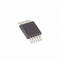
MAX4685EUB+ Maxim Integrated Products, MAX4685EUB+ Datasheet - Page 6

MAX4685EUB+
Manufacturer Part Number
MAX4685EUB+
Description
IC SWITCH DUAL SPDT 10UMAX
Manufacturer
Maxim Integrated Products
Datasheet
1.MAX4684EBCT.pdf
(10 pages)
Specifications of MAX4685EUB+
Function
Switch
Circuit
2 x SPDT
On-state Resistance
800 mOhm
Voltage Supply Source
Single Supply
Voltage - Supply, Single/dual (±)
1.8 V ~ 5.5 V
Operating Temperature
-40°C ~ 85°C
Mounting Type
Surface Mount
Package / Case
10-MSOP, Micro10™, 10-uMAX, 10-uSOP
Number Of Switches
Dual
Switch Configuration
SPDT
On Resistance (max)
0.8 Ohms
On Time (max)
60 ns
Off Time (max)
40 ns
Off Isolation (typ)
- 64 dB
Supply Voltage (max)
5.5 V
Supply Voltage (min)
1.8 V
Maximum Power Dissipation
444 mW
Maximum Operating Temperature
+ 85 C
Mounting Style
SMD/SMT
Description/function
Analog Switch
Minimum Operating Temperature
- 40 C
Off State Leakage Current (max)
10 nA
Lead Free Status / RoHS Status
Lead free / RoHS Compliant
0.5 Ω Ω /0.8 Ω Ω Low-Voltage, Dual SPDT
Analog Switches in UCSP
The MAX4684/MAX4685 are low on-resistance, low-
voltage, dual SPDT analog switches that operate from a
+1.8V to +5.5V supply. The devices are fully specified
for nominal 3V applications. The MAX4684/MAX4685
have break-before-make switching and fast switching
speeds (t
The MAX4684 offers asymmetrical normally closed
(NC) and normally open (NO) R
require asymmetrical loads (examples include speaker
headsets and internal speakers). The part features a
0.5Ω max R
for its NO switch at the 2.7V supply. The MAX4685 fea-
tures a 0.8Ω max on-resistance for both NO and NC
switches at the +2.7V supply.
The MAX4684/MAX4685 logic inputs accept up to
+5.5V regardless of supply voltage. For example, with a
+3.3V supply, IN_ may be driven low to GND and high
to 5.5V. Driving IN_ rail-to-rail minimizes power con-
sumption. Logic levels for a +1.8V supply are 0.5V (low)
and 1.4V (high).
Analog signals that range over the entire supply voltage
(V+ to GND) are passed with very little change in on-
resistance (see Typical Operating Characteristics ). The
switches are bidirectional, so the NO_, NC_, and COM_
pins can be either inputs or outputs.
6
_______________________________________________________________________________________
NAME
COM_
GND
NC_
NO_
IN_
V+
EP
ON
ON
= 50ns max, t
Applications Information
for its NC switch and a 0.8Ω max RON
A1, C1
A2, C2
A3, C3
A4, C4
UCSP
B4
B1
—
Detailed Description
OFF
Digital Control Inputs
PIN
Analog Signal Levels
= 40ns max).
µMAX/TDFN
ON
2, 10
5, 7
4, 8
3, 9
for applications that
—
1
6
Analog Switch—Normally Closed Terminal
Digital Control Input
Analog Switch—Common Terminal
Analog Switch—Normally Open Terminal
Positive Supply Voltage Input
Ground
Exposed Pad. Connect EP to GND (for TDFN only.)
Caution: Do not exceed the absolute maximum rat-
ings because stresses beyond the listed ratings
may cause permanent damage to devices.
Proper power-supply sequencing is recommended for
all CMOS devices. Always apply V+ before applying
analog signals, especially if the analog signal is not
current limited. If this sequencing is not possible, and if
the analog inputs are not current limited to <20mA, add
a small signal diode (D1) as shown in Figure 1. Adding
a protection diode reduces the analog range to a diode
drop (about 0.7V) below V+ (for D1). R
slightly at low supply voltages. Maximum supply volt-
age (V+) must not exceed +6V. Protection diode D1
also protects against some overvoltage situations. No
damage will result on Figure 1’s circuit if the supply
voltage is below the absolute maximum rating applied
to an analog signal pin.
Figure 1. Overvoltage Protection Using Two External Blocking
Diodes
V g
FUNCTION
Power-Supply Sequencing and
NO
POSITIVE SUPPLY
GND
Overvoltage Protection
V+
D1
Pin Description
COM
MAX4684
MAX4685
ON
increases


