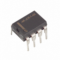
DG419DJ+ Maxim Integrated Products, DG419DJ+ Datasheet - Page 2

DG419DJ+
Manufacturer Part Number
DG419DJ+
Description
IC SWITCH SPDT 8DIP
Manufacturer
Maxim Integrated Products
Type
Analog Switchr
Datasheet
1.DG418DY.pdf
(12 pages)
Specifications of DG419DJ+
Function
Switch
Circuit
1 x SPDT
On-state Resistance
35 Ohm
Voltage Supply Source
Single, Dual Supply
Voltage - Supply, Single/dual (±)
10 V ~ 30 V, ±4.5 V ~ 20 V
Operating Temperature
-40°C ~ 85°C
Mounting Type
Through Hole
Package / Case
8-DIP (0.300", 7.62mm)
Number Of Switches
Dual
Switch Configuration
SPDT
On Resistance (max)
35 Ohms
On Time (max)
175 ns
Off Time (max)
145 ns
Off Isolation (typ)
68 dB
Supply Voltage (max)
+/- 20 V
Supply Voltage (min)
+/- 4.5 V
Supply Current
- 0.0001 uA
Maximum Power Dissipation
727 mW
Maximum Operating Temperature
+ 85 C
Mounting Style
Through Hole
Description/function
Analog Switch
Input Level
CMOS, TTL
Minimum Operating Temperature
- 40 C
Off State Leakage Current (max)
5 nA
Package
8PDIP N
Maximum On Resistance
100@10.8V Ohm
Maximum Propagation Delay Bus To Bus
175@±15V ns
Maximum High Level Output Current
30 mA
Switch Architecture
SPDT
Power Supply Type
Single|Dual
Lead Free Status / RoHS Status
Lead free / RoHS Compliant
ABSOLUTE MAXIMUM RATINGS
Voltage Referenced to V-
Digital Inputs V
Continuous Current (any terminal) (Note 1) ........................30mA
Peak Current, S or D (pulsed at 1ms, 10% duty cycle max)..100mA
Improved, SPST/SPDT Analog Switches
Note 1: Signals on S, D, or IN exceeding V+ or V- are clamped by internal diodes. Limit forward current to maximum current ratings.
Stresses beyond those listed under “Absolute Maximum Ratings” may cause permanent damage to the device. These are stress ratings only, and functional
operation of the device at these or any other conditions beyond those indicated in the operational sections of the specifications is not implied. Exposure to
absolute maximum rating conditions for extended periods may affect device reliability.
ELECTRICAL CHARACTERISTICS—Dual Supplies
(V+ = +15V, V- = -15V, V
2
SWITCH
Analog Signal Range
Drain-Source
On-Resistance
On-Resistance Match
Between Channels
(Note 4)
On-Resistance Flatness
(Note 4)
Source-Off
Leakage Current
(Note 5)
Drain-Off
Leakage Current
(Note 5)
Drain-On
Leakage Current
(Note 5)
V+ .......................................................................................44V
GND....................................................................................25V
VL ..................................................(GND - 0.3V) to (V+ + 0.3V)
_______________________________________________________________________________________
PARAMETER
S
, V
D
(Note 1) .........(V- - 2V) to (V+ + 2V) or 30mA
L
= 5V, GND = 0V, V
R
SYMBOL
∆R
R
V
FLAT(ON)
I
I
I
S(OFF)
D(OFF)
DS(ON)
D(ON)
S_
DS(ON)
, V
D
(Note 3)
V+ = 13.5V, V- = -13.5V,
V
I
V+ = 15V, V- = -15V,
V
I
V+ = 15V, V- = -15V,
V
I
V+ = 16.5V, V- = -16.5V,
V
V
V+ = 16.5V,
V- = -16.5V,
V
V
V+ = 16.5V,
V- = -16.5V,
V
V
(whichever occurs first)
S
S
S
D
D
D
D
S
D
S
D
S
INL
= -10mA
= -10mA
= -10mA
=
=
= ±15.5V
= ±10V,
= ±10V,
= ±5V,
= ±15.5V,
= ±15.5V,
= ±15.5V,
±
±
= 0.8V, V
15.5V
15.5V
INH
DG417/
DG417/
DG418
DG419
DG418
DG419
CONDITIONS
= 2.4V, T
T
T
T
T
T
T
T
T
T
T
T
T
T
T
T
T
T
T
T
T
T
A
A
A
A
A
A
A
A
A
MAX
A
A
MAX
A
A
MAX
A
A
MAX
A
A
MAX
= T
Continuous Power Dissipation (T
Operating Temperature Ranges
Storage Temperature Range .............................-65°C to +150°C
Lead Temperature (soldering, 10sec) .............................+300°C
= +25°C
= T
= +25°C
= T
= +25°C
= T
= +25°C
= T
= +25°C
= T
= +25°C
= T
= +25°C
= T
= +25°C
= T
Plastic DIP (derate 9.09mW/°C above +70°C) .............727mW
SO (derate 5.88mW/°C above +70°C) ..........................471mW
CERDIP (derate 8.00mW/°C above +70°C) ..................640mW
DG41_C_ .............................................................0°C to +70°C
DG41_D_ ..........................................................-40°C to +85°C
DG41_AK ........................................................-55°C to +125°C
MIN
MIN
MIN
MIN
MIN
MIN
MIN
MIN
MIN
to T
to T
to T
to T
to
to
to
to
to
MAX
MAX
MAX
MAX
C, D
A
C, D
A
C, D
A
C, D
A
C, D
A
, unless otherwise noted.)
C, D
A
-0.25
-0.25
-0.75
-0.75
MIN
-0.4
-15
-20
-20
-10
-40
-10
-40
-10
-40
-5
-5
A
(Note 2)
= +70°C)
TYP
-0.1
0.1
20
20
MAX
0.25
0.25
0.75
0.75
0.4
15
35
30
45
20
20
10
40
10
40
10
40
3
4
4
6
5
5
UNITS
nA
nA
nA
Ω
Ω
Ω
V


