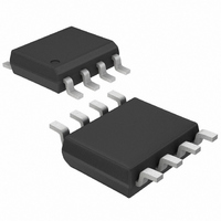
MAX325ESA+ Maxim Integrated Products, MAX325ESA+ Datasheet - Page 6

MAX325ESA+
Manufacturer Part Number
MAX325ESA+
Description
IC SWITCH DUAL SPST 8SOIC
Manufacturer
Maxim Integrated Products
Datasheet
1.MAX325CPA.pdf
(12 pages)
Specifications of MAX325ESA+
Function
Switch
Circuit
2 x SPST - NC/NO
On-state Resistance
60 Ohm
Voltage Supply Source
Single Supply
Voltage - Supply, Single/dual (±)
2.7 V ~ 16 V
Current - Supply
1µA
Operating Temperature
-40°C ~ 85°C
Mounting Type
Surface Mount
Package / Case
8-SOIC (0.154", 3.90mm Width)
Lead Free Status / RoHS Status
Lead free / RoHS Compliant
The MAX323/MAX324/MAX325 are TTL compatible
when powered from a single +5V supply. When pow-
ered from other supply voltages, TTL compatibility is
not guaranteed, and the logic inputs should be driven
from rail to rail. For example, with a 15V supply, IN1
and IN2 should be driven low to 0V and high to 15V.
Similarly, with a 3.3V supply, IN1 and IN2 should be dri-
ven low to 0V and high to 3.3V
Driving IN1 and IN2 rail-to-rail minimizes power con-
sumption.
Analog signals that range over the entire supply voltage
(V+ to GND) can be switched with very little change in
on-resistance over the entire voltage range (see Typical
Operating Characteristics ). All the switches are bidirec-
tional, so NO_, NC_, and COM_ pins can be used as
either inputs or outputs.
Do not exceed the absolute maximum ratings, because
stresses beyond the listed ratings may cause permanent
damage to the devices.
Proper power-supply sequencing is recommended for
all CMOS devices. Always apply V+ before applying
analog signals or logic inputs, especially if the analog
Precision, Single-Supply,
SPST Analog Switches
_____________________Pin Description
6
__________Applications Information
PIN
2, 6
3, 7
1
4
5
8
_______________________________________________________________________________________
IN2, IN1
COM1,
NAME
COM2
GND
NC1
NO2
NC2
NO1
V+
Normally Open Analog Switch Terminal
(MAX323/MAX325)
Normally Closed Analog Switch Terminal
(MAX324 only)
Analog Switch Common Terminal
Logic Inputs
Ground
Normally Open Analog Switch Terminal
(MAX323 only)
Normally Closed Analog Switch Terminal
(MAX324/MAX325)
Positive Supply
and Overvoltage Protection
Power-Supply Sequencing
Analog Signal Levels
FUNCTION
Logic Levels
or logic signals are not current-limited. If this sequenc-
ing is not possible, and if the analog or logic inputs are
not current-limited to <30mA, add a small-signal diode
(D1) as shown in Figure 1. If the analog signal can dip
below GND, add D2. Adding protection diodes reduces
the analog signal range to a diode-drop (about 0.7V)
below V+ (for D1), and to a diode-drop above ground
(for D2). Leakage is unaffected by adding the diodes.
On-resistance increases by a small amount at low sup-
ply voltages. Maximum supply voltage (V+) must not
exceed 17V.
Adding protection diodes causes the logic thresholds
to be shifted relative to the power-supply rails. This can
be significant when low supply voltages (5V or less) are
used. With a 5V supply, TTL compatibility is not guaran-
teed when protection diodes are added. Driving IN1
and IN2 all the way to the supply rails (i.e. to a diode-
drop higher than the V+ pin, or to a diode-drop lower
than the GND pin) is always acceptable.
Protection diodes D1 and D2 also protect against
some overvoltage situations. With Figure 1’s circuit, if
the supply voltage is below the absolute maximum rat-
ing, and if a fault voltage up to the absolute maximum
rating is applied to an analog signal pin, no damage
will result. For example, with a +5V supply, analog sig-
nals up to ±8V will not damage the circuit of Figure 1.
If only a single fault signal is present, the fault voltage
can rise to +17V or to -12V without damage occurring.
Figure 1. Overvoltage Protection Using Two External Blocking
Diodes
V g
NO
POSITIVE SUPPLY
GND
V+
D1
D2
COM


