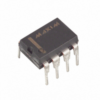
MAX319CPA+ Maxim Integrated Products, MAX319CPA+ Datasheet - Page 4

MAX319CPA+
Manufacturer Part Number
MAX319CPA+
Description
IC SWITCH SPDT 8DIP
Manufacturer
Maxim Integrated Products
Type
Analog Switchr
Datasheet
1.MAX318CPA.pdf
(12 pages)
Specifications of MAX319CPA+
Function
Switch
Circuit
1 x SPDT
On-state Resistance
35 Ohm
Voltage Supply Source
Single, Dual Supply
Voltage - Supply, Single/dual (±)
10 V ~ 30 V, ±4.5 V ~ 20 V
Current - Supply
1µA
Operating Temperature
0°C ~ 70°C
Mounting Type
Through Hole
Package / Case
8-DIP (0.300", 7.62mm)
Number Of Switches
Dual
Switch Configuration
SPDT
On Resistance (max)
35 Ohms
On Time (max)
175 ns
Off Time (max)
145 ns
Off Isolation (typ)
68 dB
Supply Voltage (max)
+/- 20 V
Supply Voltage (min)
+/- 4.5 V
Supply Current
0.0001 uA
Maximum Power Dissipation
471 mW
Maximum Operating Temperature
+ 70 C
Mounting Style
Through Hole
Description/function
Analog Switch
Input Level
CMOS, TTL
Minimum Operating Temperature
0 C
Off State Leakage Current (max)
10 nA
Package
8PDIP N
Maximum On Resistance
100@10.8V Ohm
Maximum Propagation Delay Bus To Bus
175@±15V ns
Maximum High Level Output Current
30 mA
Maximum Turn-off Time
40(Typ)@12V ns
Maximum Turn-on Time
110(Typ)@12V ns
Switch Architecture
SPDT
Power Supply Type
Single|Dual
Lead Free Status / RoHS Status
Lead free / RoHS Compliant
ELECTRICAL CHARACTERISTICS — Single Supply
(V+ = 12V, V- = 0V, V
Note 2: Typical values are for design aid only, not guaranteed, not subject to production testing.
Note 3: Guaranteed by design.
Note 4: On resistance match between channels and flatness are guaranteed only with bipolar-supply operation.
Note 5: Off Isolation = 20log
Note 6: Between any two switches.
Precision, CMOS Analog Switches
4
SWITCH
Analog-Signal Range
Drain-Source On Resistance
DYNAMIC
Turn-On Time
Turn-Off Time
Break-Before-Make
Time Delay
Charge Injection
SUPPLY
Positive Supply Current
Negative Supply Current
Logic Supply Current
Ground Current
_______________________________________________________________________________________
PARAMETER
L
= 5V, GND = 0V, V
10
(
V
SYMBOL
V
NC
NO,
V
V
R
I
t
COM,
t
GND
COM
OFF
(ON)
ON
I+
t
Q
I
I-
or V
D
L
INH
V
NC
NO
= 2.4V, V
(Note 3)
I
V
V
MAX319, R
Figure 4
C
Figure 5
V+ = 13.2V, all channels on or off,
V
V+ = 13.2V, all channels on or off,
V
V
V
V
V
)
(NC or NO)
COM
COM
IN
IN
L
IN
L
IN
L
, V
= 5.25V, all channels on or off,
= 5.25V, all channels on or off,
= 10nF, V
= 0V or 5V, V
= 0V or 5V, V
= 0V or 5V
= 0V or 5V
COM
INL
= 8V, Figure 2
= 8V, Figure 2
= 0.8V, T
= output, V
= -10mA, V
L
= 1000Ω, C
GEN
CONDITIONS
L
L
A
= 0V, R
= 5.25V
= 5.25V
= +25°C, unless otherwise noted.)
NC
COM
or V
L
GEN
= 35pF,
= 3.8V, V+ = 10.8V
NO
= 0V,
= input to off switch.
MIN
0
(Note 2)
-0.0001
0.0001
0.0001
0.0001
TYP
110
40
40
60
2
MAX
100
12
10
UNITS
pC
µA
µA
µA
µA
ns
ns
ns
Ω
V


