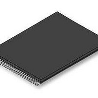
S29GL128S10TFI020 Spansion Inc., S29GL128S10TFI020 Datasheet - Page 70

S29GL128S10TFI020
Manufacturer Part Number
S29GL128S10TFI020
Description
Flash 128 MBIT 3V 100NS PAGE MODE FLASH
Manufacturer
Spansion Inc.
Datasheet
1.S29GL128S10TFI020.pdf
(97 pages)
Specifications of S29GL128S10TFI020
Data Bus Width
16 bit
Memory Type
Flash
Memory Size
128 Mbit
Architecture
Uniform
Timing Type
Asynchronous
Interface Type
CFI
Access Time
100 ns
Supply Voltage (max)
3.6 V
Supply Voltage (min)
2.7 V
Maximum Operating Current
100 mA
Operating Temperature
- 40 C to + 85 C
Mounting Style
SMD/SMT
Package / Case
TSOP-56
Lead Free Status / Rohs Status
Compliant
Available stocks
Company
Part Number
Manufacturer
Quantity
Price
Company:
Part Number:
S29GL128S10TFI020
Manufacturer:
SPANSION
Quantity:
101
Company:
Part Number:
S29GL128S10TFI020
Manufacturer:
SPANSION
Quantity:
1 001
Part Number:
S29GL128S10TFI020
Manufacturer:
SPANSION
Quantity:
20 000
9.
9.1
9.2
9.3
70
9.3.1
9.3.2
9.3.3
Electrical Specifications
Absolute Maximum Ratings
Latchup Characteristics
Operating Ranges
Temperature Ranges
Power Supply Voltages
Power-Up and Power-Down
Notes:
1. Minimum DC voltage on input or I/O pins is -0.5V. During voltage transitions, input or I/O pins may undershoot V
2. No more than one output may be shorted to ground at a time. Duration of the short circuit should not be greater than one second.
3. Stresses above those listed under
This product complies with JEDEC standard JESD78C latchup testing requirements.
Industrial (I) Devices
V
V
Operating ranges define those limits between which the functionality of the device is guaranteed.
V
200 mV (V
The device ignores all inputs until a time delay of t
rise above, and stay above, the minimum V
on reset operations.
During power-down or voltage drops below V
drop below V
again rise to their operating ranges. See
V
the part locks up from improper initialization, a hardware reset can be used to initialize the part correctly.
Normal precautions must be taken for supply decoupling to stabilize the V
device in a system should have the V
the package connections (this capacitor is generally on the order of 0.1 µF).
Storage Temperature Plastic Packages
Ambient Temperature with Power Applied
Voltage with Respect to Ground
All pins
Output Short Circuit Current
V
V
CC
IO
CC
LKO
CC
IO
up to 20 ns. See
V
functional operation of the device at these or any other conditions above those indicated in the operational sections of this data sheet is
not implied. Exposure of the device to absolute maximum rating conditions for extended periods may affect device reliability.
CC
Ambient Temperature (T
must always be greater than or equal to V
maximum the part will stay initialized and will work correctly when V
+0.5V. During voltage transitions, input or I/O pins may overshoot to V
(Note 1)
IO
≥ V
CC
Figure 9.3 on page
Reset (V
CC
- 200 mV) when V
(Note 2)
D a t a
RST
1.65V to V
) minimum for a period of t
A
Absolute Maximum Ratings
)
72. Maximum DC voltage on input or I/O pins is
S h e e t
GL-S MirrorBit
-40°C to +85°C
Table 9.1 Absolute Maximum Ratings
CC
2.7V to 3.6V
CC
IO
+ 200 mV
is below the V
Figure 9.2 on page
and V
CC
CC
( A d v a n c e
and V
IO
IO
®
Lockout maximum (V
power supplies decoupled by a suitable capacitor close to
(V
Family
VCS
CC
may cause permanent damage to the device. This is a stress rating only;
IO
thresholds. During t
has elapsed after the moment that V
≥ V
IO
PD
minimum.
IO
for the part to initialize correctly when V
). V
71. If during a voltage drop the V
CC
+2.0V for periods up to 20 ns. See
IO
I n f o r m a t i o n )
S29GL_128S_01GS_00_01 February 11, 2011
must track the rise and fall of V
LKO
CC
), the V
VCS
CC
-0.5 V to (V
is again above V
-65°C to +150°C
-65°C to +125°C
-0.5 V to +4.0 V
-0.5 V to +4.0 V
and V
the device is performing power
100 mA
CC
IO
CC
and V
power supplies. Each
+ 0.5 V)
SS
IO
Figure 9.4 on page 72
CC
to -2.0V for periods of
voltages must
CC
CC
and V
minimum. If
stays above
CC
CC
IO
within
and V
both
IO


