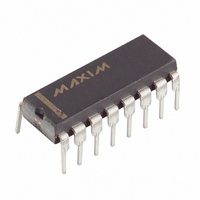
MAX303CPE+ Maxim Integrated Products, MAX303CPE+ Datasheet - Page 3

MAX303CPE+
Manufacturer Part Number
MAX303CPE+
Description
IC SWITCH DUAL SPDT 16DIP
Manufacturer
Maxim Integrated Products
Datasheet
1.MAX303CPE.pdf
(8 pages)
Specifications of MAX303CPE+
Function
Switch
Circuit
2 x SPDT
On-state Resistance
35 Ohm
Voltage Supply Source
Single, Dual Supply
Voltage - Supply, Single/dual (±)
10 V ~ 30 V, ±4.5 V ~ 20 V
Operating Temperature
0°C ~ 70°C
Mounting Type
Through Hole
Package / Case
16-DIP (0.300", 7.62mm)
Number Of Switches
Dual
Switch Configuration
SPDT
On Resistance (max)
35 Ohms
On Time (max)
150 ns
Off Time (max)
100 ns
Off Isolation (typ)
72 dB
Supply Voltage (max)
+/- 20 V
Supply Voltage (min)
+/- 4.5 V
Supply Current
0.01 uA
Maximum Power Dissipation
842 mW
Maximum Operating Temperature
+ 70 C
Mounting Style
Through Hole
Description/function
Analog Switch
Input Level
CMOS
Minimum Operating Temperature
0 C
Off State Leakage Current (max)
0.5 nA
Lead Free Status / RoHS Status
Lead free / RoHS Compliant
Note 2: The algebraic convention, where the most negative value is a minimum and the most positive value a maximum, is used on
Note 3: Guaranteed by design.
Note 4:
Note 5: See Figure 4. Off isolation = 20log
Note 6: Between any two switches. See Figure 5.
ELECTRICAL CHARACTERISTICS (continued)
(V+ = 15V, V- = -15V, V
INPUT
Input Current with
Input-Voltage High
Input Current with
Input-Voltage Low
SUPPLY
Power-Supply Range
Positive Supply Current
Negative Supply Current
Logic-Supply Current
Ground Current
DYNAMIC
Turn-On Time
Turn-Off Time
Break-Before-Make
Time Delay (Note 3)
Charge Injection
(Note 3)
Off-Isolation (Note 5)
Crosstalk (Note 6)
Off-Capacitance
COM Off-Capacitance
Channel-On Capacitance
Precision, Dual, High-Speed Analog Switches
PARAMETER
this data sheet.
specified voltages.
R
ON
= R
ON
_________________________________________________________________________________________________ 3
MAX - R
L
= +5V, GND = 0V, V
C
C
SYMBOL
COM(OFF
COM(ON)
OIRR
I
C
t
ON
I
I
GND
t
INH
INH
OFF
I+
ON
t
Q
OF
I-
I
D
L
MIN. On resistance match between channels and flatness are guaranteed only with
All channels on or off,
V
V+ = 16.5V, V- = -16.5V
All channels on or off,
V
V+ = 16.5V, V- = -16.5V
All channels on or off,
V
V+ = 16.5V, V- = -16.5V
All channels on or off,
V
V+ = 16.5V, V- = -16.5V
f = 1MHz, Figure 6
V
V
Figure1
Figure 1
MAX303 only,
Figure 2
C
R
Figure 3
R
f = 1MHz, Figure 4
R
f = 1MHz, Figure 5
f = 1MHz, Figure 6
f = 1MHz, Figure 7
10
IN
IN
IN
IN
IN
IN
GEN
L
L
L
INH
V
_ = 2.4V, all others = 0.8V
_ = 0.8V, all others = 2.4V
= 10nF, V
= 100Ω, C
= 50Ω, C
= 0V or 5V,
= 0V or 5V,
= 0V or 5V,
= 0V or 5V,
COM
= 0Ω,
= +2.4V, V
/V
NC or
L
GEN
L
= 5pF,
V
= 5pF,
NO
INL
= 0V,
, V
CONDITIONS
= +0.8V, T
COM
= output, V
T
T
T
T
T
T
T
T
T
T
T
T
T
T
T
T
T
A
A
A
A
A
A
A
A
A
A
A
A
A
A
A
A
A
= +25°C
= T
= +25°C
= T
= +25°C
= T
= +25°C
= T
= +25°C
= +25°C
= +25°C
= +25°C
= +25°C
= +25°C
= +25°C
A
= +25°C
= +25°C
= T
MIN
MIN
MIN
MIN
MIN
to T
to T
to T
to T
NC or
to T
MAX
MAX
MAX
MAX
V
MAX
NO
, unless otherwise noted.)
= input to off switch.
-1.000 0.005 1.000
-1.000 0.005 1.000
-1.00
-5.00
-1.00
-5.00
-1.00
-5.00
-1.00
-5.00
±4.5
MIN
10
(Note 2)
-0.01
-0.01
TYP
0.01
0.01
100
60
20
10
72
90
39
12
12
MAX
1.00
5.00
1.00
5.00
1.00
5.00
1.00
5.00
±20
150
100
15
UNITS
µA
µA
µA
µA
µA
µA
pC
dB
dB
ns
ns
ns
pF
V
pF
pF


