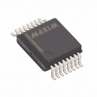
MAX4590CAE+ Maxim Integrated Products, MAX4590CAE+ Datasheet - Page 5

MAX4590CAE+
Manufacturer Part Number
MAX4590CAE+
Description
IC SWITCH DUAL SPST 16SSOP
Manufacturer
Maxim Integrated Products
Datasheet
1.MAX4590CAE.pdf
(12 pages)
Specifications of MAX4590CAE+
Function
Switch
Circuit
2 x SPST - NO
On-state Resistance
1.25 Ohm
Voltage Supply Source
Single, Dual Supply
Voltage - Supply, Single/dual (±)
4.5 V ~ 36 V, ±4.5 V ~ 20 V
Operating Temperature
0°C ~ 70°C
Mounting Type
Surface Mount
Package / Case
16-SSOP
Lead Free Status / RoHS Status
Lead free / RoHS Compliant
ELECTRICAL CHARACTERISTICS—Single Supply (continued)
(V+ = +12V, V- = 0, V
T
Note 2: The algebraic convention, where the most negative value is a minimum and the most positive value a maximum, is used in
Note 3: Guaranteed by design.
Note 4: ∆R
Note 5: Flatness is defined as the difference between the maximum and minimum value of on-resistance as measured over the
Note 6: Leakage parameters are 100% tested at maximum-rated hot temperature and guaranteed by correlation at +25°C.
Note 7: Off-isolation = 20 log
Note 8: Between any two switches.
Note 9: Leakage testing at single supply is guaranteed by testing with dual supplies.
(Circuit of Figure 1, T
SWITCH DYNAMIC CHARACTERISTICS
A
Turn-On Time
Turn-Off Time
Charge Injection
Crosstalk (Note 8)
NC_ or NO_ Capacitance
COM Off-Capacitance
On-Capacitance
= +25°C.)
2.5
2.0
1.5
1.0
0.5
0
-20
this data sheet.
specified analog signal range.
PARAMETER
V+, V- = ±5.0V
-16
ON
ON-RESISTANCE vs. V
-12 -8
= R
V+, V- = ±15.0V
(DUAL SUPPLIES)
ON(MAX)
-4
_______________________________________________________________________________________
A
V
COM
= +25°C, unless otherwise noted.)
L
0
= +5V, V
(V)
V+, V- = ±20.0V
- R
4
10
ON(MIN)
8
[V
COM
12 16 20
COM
IN_H
SYMBOL
.
C
C
C
/ (V
(COM)_
(COM)_
t
(OFF)_
V
= 2.4V, V
t
OFF
ON
Q
CT
NC
or V
NO
1.2
1.1
1.0
0.9
0.8
0.7
0.6
0.5
0.4
IN_L
V
V
C
Figure 3, T
R
Figure 5, T
f = 1MHz, Figure 6, T
f = 1MHz, Figure 6, T
f = 1MHz, Figure 7, T
-15
COM_
COM_
)], V
L
L
AND TEMPERATURE (DUAL SUPPLIES)
= 1.0nF, V
= 50Ω, C
= 0.8V, T
-12 -9 -6
COM
= +10V, Figure 2, T
= +10V, Figure 2, T
ON-RESISTANCE vs. V
= output, V
A
A
L
= +25°C
= +25°C
GEN
T
T
T
A
CONDITIONS
= 5pF, f = 1MHz,
A
A
A
-3
= +85°C
= +25°C
V
= -40°C
= T
CMOS Analog Switches
COM
= 0, R
0
Typical Operating Characteristics
MIN
(V)
A
A
A
3
NC
V+, V- = ±15V
= +25°C
= +25°C
= +25°C
to T
GEN
6
or V
COM
A
A
9
MAX
= +25°C
= +25°C
= 0,
NO
12
= input to off switch.
1.25Ω, Dual SPST,
, unless otherwise noted. Typical values are at
15
5
4
3
2
1
0
MIN
0
2
4
ON-RESISTANCE vs. V
(Note 2)
6
V+ = +5V
V+ = +12V
V+ = +24V
TYP
150
200
175
175
275
-65
(SINGLE SUPPLY)
40
8
10
V
COM
12
(V)
MAX
14
16
18
COM
UNITS
20
V- = 0
pC
dB
pF
pF
pF
ns
ns
22
24
5


