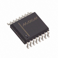
MAX355CWE+ Maxim Integrated Products, MAX355CWE+ Datasheet - Page 8

MAX355CWE+
Manufacturer Part Number
MAX355CWE+
Description
IC MULTIPLEXER DUAL 4X1 16SOIC
Manufacturer
Maxim Integrated Products
Datasheet
1.MAX355CWE.pdf
(12 pages)
Specifications of MAX355CWE+
Function
Multiplexer
Circuit
2 x 4:1
On-state Resistance
350 Ohm
Voltage Supply Source
Single, Dual Supply
Voltage - Supply, Single/dual (±)
4.5 V ~ 36 V, ±4.5 V ~ 18 V
Operating Temperature
0°C ~ 70°C
Mounting Type
Surface Mount
Package / Case
16-SOIC (0.300", 7.50mm Width)
Lead Free Status / RoHS Status
Lead free / RoHS Compliant
Fault-Protected Analog Multiplexers
Figure 5. Off Isolation
Figure 7. NO/COM Capacitance
Maxim’s MAX354/MAX355 are fully fault protected for
continuous input voltages up to ±40V, whether or not
the V+ and V- power supplies are present. These
devices use a “series FET” protection scheme that not
only protects the multiplexer output from overvoltage,
but also limits the input current to sub-microamp levels.
When signal voltages exceed or are within approxi-
mately 1.5V of the supply rails, on-resistance increas-
es. This greater on-resistance limits fault currents and
output voltage, protecting sensitive circuits and com-
ponents. The protected output clamps at approximately
8
_________________________________Test Circuits/Timing Diagrams (continued)
_______________Detailed Description
CHANNEL
_______________________________________________________________________________________
SELECT
V
R
IN
S
= 50
A2
A1
A0
GND
MAX354
A0
A1
A2
NO1
NO8
EN
+15V
Fault-Protection Circuitry
V+
GND
-15V
MAX354
10nF
V-
EN
+15V
COM
V+
NO1
NO8
OFF ISOLATION = 20log
-15V
COM
10nF
V-
CAPACITANCE
R
1k
ANALYZER
f = 1MHz
L
1MHz
V
OUT
V
V
OUT
IN
1.5V below the supply rails and maintains the correct
polarity. There are no glitches or polarity reversals
going into or coming out of a fault condition.
Figures 8 and 9 show how the series FET circuit protects
against overvoltage conditions. When power is off, the
gates of all three FETs are at ground. With a -25V input,
N-channel FET Q1 is turned on by the +25V gate-to-
source voltage. The P-channel device (Q2), however,
has +25V V
input signal from reaching the output. If the input volt-
age is +25V, Q1 has a negative V
Similarly, only sub-microamp leakage currents can flow
from the output back to the input, since any voltage will
turn off either Q1 or Q2.
Figure 6. Crosstalk
R = 1k
R
G
= 50
GS
V
IN
and is turned off, thereby preventing the
A0
A1
A2
NO1
NO2
NO8
GND
MAX354
10nF
EN
+15V
V+
GS
10nF
-15V
COM
, which turns it off.
CROSSTALK = 20log
V-
R
1k
L
V
OUT
V
V
OUT
IN


