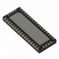
PI2PCIE412-DZHE Pericom Semiconductor, PI2PCIE412-DZHE Datasheet - Page 2

PI2PCIE412-DZHE
Manufacturer Part Number
PI2PCIE412-DZHE
Description
IC MUX/DEMUX QUAD 2X1 42TQFN
Manufacturer
Pericom Semiconductor
Datasheet
1.PI2PCIE412-DZHE.pdf
(9 pages)
Specifications of PI2PCIE412-DZHE
Function
Multiplexer/Demultiplexer
Circuit
4 x 2:1
Voltage Supply Source
Single Supply
Voltage - Supply, Single/dual (±)
1.5 V ~ 2 V
Current - Supply
200µA
Operating Temperature
-40°C ~ 85°C
Mounting Type
Surface Mount
Package / Case
42-TQFN
Number Of Channels
4 Channel
On Time (max)
8 ns @ 1.8 V @ - 40 C to 85 C
Off Time (max)
4 ns @ 1.8 V @ - 40 C to 85 C
Supply Voltage (max)
2 V
Supply Voltage (min)
1.5 V
Maximum Power Dissipation
500 mW
Maximum Operating Temperature
+ 85 C
Minimum Operating Temperature
- 40 C
Mounting Style
SMD/SMT
Supply Voltage Range
1.5V To 2V
Operating Temperature Range
-40°C To +85°C
Digital Ic Case Style
TQFN
No. Of Pins
42
Filter Terminals
SMD
Communication Function
Switch
No. Of Channels
4
Rohs Compliant
Yes
Dc
0716
Lead Free Status / RoHS Status
Lead free / RoHS Compliant
Available stocks
Company
Part Number
Manufacturer
Quantity
Price
Part Number:
PI2PCIE412-DZHEX
Manufacturer:
PERICOM
Quantity:
20 000
Maximum Ratings
(Above which useful life may be impaired. For user guidelines, not tested.)
DC Electrical Characteristics for Switching over Operating Range
Power Supply Characteristics
Dynamic Electrical Characteristics Over the Operating Range
Notes:
1.
2.
I
X
O
V IH
V IL
V IK
I IH
I IL
Parameters
Storage Temperature ....................................................–65°C to +150°C
Supply Voltage to Ground Potential ................................–0.5V to +2.5V
DC Input Voltage ...............................................................–0.5V to V
DC Output Current ....................................................................... 120mA
Power Dissipation ........................................................................... 0.5W
CC
Paramenter
Parameter
TALK
IRR
For Max. or Min. conditions, use appropriate value specified under Electrical Characteristics for the applicable device type.
Typical values are at V
Quiescent Power Supply Current
Crosstalk
OFF Isolation
Input HIGH Voltage
Input LOW Voltage
Clamp Diode Voltage
Input HIGH Current
Input LOW Current
Description
CC
= 1.8V, T
Description
Description
A
= 25°C ambient and maximum loading.
See Fig. 1 for Measurement Setup, f = 10 MHz
See Fig. 2 for Measurement Setup, f = 10 MHz
Guaranteed HIGH level
Guaranteed LOW level
V
V
V
Test Conditions
CC
CC
CC
V
CC
= Max., I
= Max., V
= Max., V
Test Conditions
= Max., V
2
IN
Test Conditions
IN
IN
= –18mA
CC
= V
= GND
IN
4-Differential Channel, 2:1 Mux/DeMux Switch
= GND or V
CC
(1)
Note: Stresses greater than those listed under MAXIMUM
RATINGS may cause permanent damage to the device. This
is a stress rating only and functional operation of the device
at these or any other conditions above those indicated in the
operational sections of this specification is not implied. Expo-
sure to absolute maximum rating conditions for extended
periods may affect reliability.
(T A = -40º to +85ºC, V CC = 1.8V±10%, GND=0V)
Enhanced, 1.8V, PCI Express Compliant,
(1)
(T
CC
A
0.65 x V
= –40°C to +85°C, V
Min.
Min
–0.5
Min.
CC
Typ.
Typ
-65
-65
–0.7
Typ.
(2)
200
(2)
(2)
CC
0.35 x V
Max.
PS8788B
PI2PCIE412-D
= 1.5V to 2.0V)
Max
–1.2
Max.
±5
±5
CC
Units
dB
Units
Units
µA
01/23/06
µA
V


