MC74HC4051ANG ON Semiconductor, MC74HC4051ANG Datasheet - Page 3
MC74HC4051ANG
Manufacturer Part Number
MC74HC4051ANG
Description
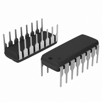
IC MUX/DEMUX 8X1 16DIP
Manufacturer
ON Semiconductor
Series
74HCr
Type
Analog Multiplexerr
Datasheet
1.MC74HC4053ANG.pdf
(18 pages)
Specifications of MC74HC4051ANG
Function
Multiplexer/Demultiplexer
Circuit
1 x 8:1
On-state Resistance
100 Ohm
Voltage Supply Source
Single, Dual Supply
Voltage - Supply, Single/dual (±)
±2 V ~ 6 V, 2 V ~ 12 V
Current - Supply
40µA
Operating Temperature
-55°C ~ 125°C
Mounting Type
Through Hole
Package / Case
16-DIP (0.300", 7.62mm)
On Resistance (max)
190 Ohms
Propagation Delay Time
40 ns
On Time (max)
245 ns
Off Time (max)
160 ns
Supply Voltage (max)
6 V
Supply Voltage (min)
2 V
Maximum Power Dissipation
750 mW
Maximum Operating Temperature
+ 125 C
Minimum Operating Temperature
- 55 C
Mounting Style
Through Hole
Number Of Switches
Single
Number Of Channels
1 Channel
Number Of Lines (input / Output)
8 / 1
Lead Free Status / RoHS Status
Lead free / RoHS Compliant
Other names
MC74HC4051ANGOS


Î Î Î Î Î Î Î Î Î Î Î Î Î Î Î Î Î Î Î Î Î Î Î
Î Î Î Î
Î Î Î Î
Î Î Î Î
Î Î Î Î
Î Î Î Î
Î Î Î Î
Î Î Î Î
Î Î Î Î
Î Î Î Î
Î Î Î Î
Î Î Î Î
Î Î Î Î
Î Î Î Î
Î Î Î Î
Î Î Î Î
Î Î Î Î
Î Î Î Î
Î Î Î Î
Î Î Î Î
Î Î Î Î
Î Î Î Î
Î Î Î Î
Stresses exceeding Maximum Ratings may damage the device. Maximum Ratings are stress
ratings only. Functional operation above the Recommended Operating Conditions is not implied.
Extended exposure to stresses above the Recommended Operating Conditions may affect
device reliability.
†Derating — Plastic DIP: – 10 mW/_C from 65_ to 125_C
For high frequency or heavy load considerations, see Chapter 2 of the ON Semiconductor High-Speed CMOS Data Book (DL129/D).
MAXIMUM RATINGS
Symbol
CHANNEL‐SELECT
V
V
INPUTS/OUTPUTS
T
V
V
P
T
CC
stg
EE
I
IS
in
D
L
Triple Single-Pole, Double-Position Plus Common Off
NOTE: This device allows independent control of each switch.
Channel-Select Input A controls the X-Switch, Input B controls
the Y-Switch and Input C controls the Z-Switch
Î Î Î Î Î Î Î Î Î Î Î Î Î Î
Î Î Î Î Î Î Î Î Î Î Î Î Î Î
Î Î Î Î Î Î Î Î Î Î Î Î Î Î
Î Î Î Î Î Î Î Î Î Î Î Î Î Î
Î Î Î Î Î Î Î Î Î Î Î Î Î Î
Î Î Î Î Î Î Î Î Î Î Î Î Î Î
Î Î Î Î Î Î Î Î Î Î Î Î Î Î
Î Î Î Î Î Î Î Î Î Î Î Î Î Î
Î Î Î Î Î Î Î Î Î Î Î Î Î Î
Î Î Î Î Î Î Î Î Î Î Î Î Î Î
Î Î Î Î Î Î Î Î Î Î Î Î Î Î
Î Î Î Î Î Î Î Î Î Î Î Î Î Î
Î Î Î Î Î Î Î Î Î Î Î Î Î Î
Î Î Î Î Î Î Î Î Î Î Î Î Î Î
Î Î Î Î Î Î Î Î Î Î Î Î Î Î
Î Î Î Î Î Î Î Î Î Î Î Î Î Î
Î Î Î Î Î Î Î Î Î Î Î Î Î Î
Î Î Î Î Î Î Î Î Î Î Î Î Î Î
Î Î Î Î Î Î Î Î Î Î Î Î Î Î
Î Î Î Î Î Î Î Î Î Î Î Î Î Î
Î Î Î Î Î Î Î Î Î Î Î Î Î Î
Î Î Î Î Î Î Î Î Î Î Î Î Î Î
ANALOG
Positive DC Supply Voltage
Negative DC Supply Voltage (Referenced to GND)
Analog Input Voltage
Digital Input Voltage (Referenced to GND)
DC Current, Into or Out of Any Pin
Power Dissipation in Still Air,
Storage Temperature Range
Lead Temperature, 1 mm from Case for 10 Seconds
INPUTS
EIAJ/SOIC Package: – 7 mW/_C from 65_ to 125_C
TSSOP Package: - 6.1 mW/_C from 65_ to 125_C
ENABLE
X0
X1
Y0
Y1
Z0
Z1
A
B
C
12
13
10
11
2
1
5
3
9
6
Plastic DIP, SOIC or TSSOP Package
LOGIC DIAGRAM
MC74HC4053A
Parameter
MC74HC4051A, MC74HC4052A, MC74HC4053A
X SWITCH
Y SWITCH
Z SWITCH
EIAJ/SOIC Package†
(Referenced to GND)
(Referenced to V
TSSOP Package†
Plastic DIP†
PIN 16 = V
PIN 7 = V
PIN 8 = GND
14
15
4
http://onsemi.com
X
Y
Z
EE
EE
CC
COMMON
OUTPUTS/INPUTS
)
Î Î Î Î Î
Î Î Î Î Î
Î Î Î Î Î
Î Î Î Î Î
Î Î Î Î Î
Î Î Î Î Î
Î Î Î Î Î
Î Î Î Î Î
Î Î Î Î Î
Î Î Î Î Î
Î Î Î Î Î
Î Î Î Î Î
Î Î Î Î Î
Î Î Î Î Î
Î Î Î Î Î
Î Î Î Î Î
Î Î Î Î Î
Î Î Î Î Î
Î Î Î Î Î
Î Î Î Î Î
Î Î Î Î Î
Î Î Î Î Î
– 0.5 to V
3
– 0.5 to + 14.0
– 0.5 to + 7.0
– 7.0 to + 5.0
– 65 to + 150
V
V
EE
CC
Value
± 25
750
500
450
260
- 0.5 to
+ 0.5
CC
+ 0.5
Î Î Î
Î Î Î
Î Î Î
Î Î Î
Î Î Î
Î Î Î
Î Î Î
Î Î Î
Î Î Î
Î Î Î
Î Î Î
Î Î Î
Î Î Î
Î Î Î
Î Î Î
Î Î Î
Î Î Î
Î Î Î
Î Î Î
Î Î Î
Î Î Î
Î Î Î
X = Don't Care
V
Enable
Y1
16
CC
1
Unit
mW
FUNCTION TABLE - MC74HC4053A
mA
_C
_C
H
L
L
L
L
L
L
L
L
V
V
V
V
Pinout: MC74HC4053A (Top View)
Control Inputs
Y0
15
Y
2
C
H
H
H
H
X
L
L
L
L
Z1
14
circuitry to guard against damage
due to high static voltages or electric
fields. However, precautions must
be taken to avoid applications of any
voltage higher than maximum rated
voltages to this high-impedance cir‐
cuit. For proper operation, V
V
range GND v (V
tied to an appropriate logic voltage
level (e.g., either GND or V
Unused outputs must be left open.
X
3
out
Select
B
H
H
H
H
L
L
L
L
X
This device contains protection
Unused inputs must always be
should be constrained to the
X1
13
4
Z
A
H
H
H
H
X
L
L
L
L
X0
12
Z0 Enable V
5
Z0
Z0
Z0
Z0
Z1
Z1
Z1
Z1
in
ON Channels
11
or V
A
6
NONE
out
Y0
Y0
Y1
Y1
Y0
Y0
Y1
Y1
10
) v V
B
7
EE
in
GND
CC
and
CC
X0
X1
X0
X1
X0
X1
X0
X1
C
9
8
).
.
Related parts for MC74HC4051ANG
Image
Part Number
Description
Manufacturer
Datasheet
Request
R

Part Number:
Description:
ON Semiconductor [VOLTAGE REGULATOR]
Manufacturer:
ON Semiconductor
Datasheet:
Part Number:
Description:
357-036-542-201 CARDEDGE 36POS DL .156 BLK LOPRO
Manufacturer:
ON Semiconductor
Datasheet:
Part Number:
Description:
357-036-542-201 CARDEDGE 36POS DL .156 BLK LOPRO
Manufacturer:
ON Semiconductor
Datasheet:
Part Number:
Description:
357-036-542-201 CARDEDGE 36POS DL .156 BLK LOPRO
Manufacturer:
ON Semiconductor
Datasheet:
Part Number:
Description:
357-036-542-201 CARDEDGE 36POS DL .156 BLK LOPRO
Manufacturer:
ON Semiconductor
Datasheet:
Part Number:
Description:
357-036-542-201 CARDEDGE 36POS DL .156 BLK LOPRO
Manufacturer:
ON Semiconductor
Datasheet:
Part Number:
Description:
357-036-542-201 CARDEDGE 36POS DL .156 BLK LOPRO
Manufacturer:
ON Semiconductor
Datasheet:
Part Number:
Description:
357-036-542-201 CARDEDGE 36POS DL .156 BLK LOPRO
Manufacturer:
ON Semiconductor
Datasheet:
Part Number:
Description:
357-036-542-201 CARDEDGE 36POS DL .156 BLK LOPRO
Manufacturer:
ON Semiconductor
Datasheet:
Part Number:
Description:
357-036-542-201 CARDEDGE 36POS DL .156 BLK LOPRO
Manufacturer:
ON Semiconductor
Datasheet:
Part Number:
Description:
357-036-542-201 CARDEDGE 36POS DL .156 BLK LOPRO
Manufacturer:
ON Semiconductor
Datasheet:
Part Number:
Description:
Manufacturer:
ON Semiconductor
Datasheet:
Part Number:
Description:
Manufacturer:
ON Semiconductor
Datasheet:
Part Number:
Description:
Manufacturer:
ON Semiconductor
Datasheet: