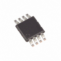
MAX4731EUA+ Maxim Integrated Products, MAX4731EUA+ Datasheet - Page 8

MAX4731EUA+
Manufacturer Part Number
MAX4731EUA+
Description
IC SWITCH DUAL SPST 8UMAX
Manufacturer
Maxim Integrated Products
Datasheet
1.MAX4733EUA.pdf
(14 pages)
Specifications of MAX4731EUA+
Function
Switch
Circuit
2 x SPST - NO
On-state Resistance
25 Ohm
Voltage Supply Source
Single Supply
Voltage - Supply, Single/dual (±)
2 V ~ 11 V
Current - Supply
0.0001µA
Operating Temperature
-40°C ~ 85°C
Mounting Type
Surface Mount
Package / Case
8-TSSOP, 8-MSOP (0.118", 3.00mm Width)
Lead Free Status / RoHS Status
Lead free / RoHS Compliant
Analog signals that range over the entire supply voltage
(GND to V+) pass with very little change in R
Typical Operating Characteristics). The bidirectional
switches allow NO_, NC_, and COM_ connections to be
used as either inputs or outputs.
CAUTION: Do not exceed the absolute maximum
ratings. Stresses beyond the listed ratings can
cause permanent damage to the devices.
Proper power-supply sequencing is recommended for
all CMOS devices. Always apply V+ before applying
analog signals, especially if the analog signal is not
current limited. If this sequencing is not possible, and if
the analog inputs are not current limited to < 20mA,
add a small-signal diode, D1, as shown in Figure 1. If
the analog signal can dip below GND, add D2. Adding
protection diodes reduces the analog signal range to a
diode drop (about 0.7V) below V+ (for D1), and to a
diode drop above ground (for D2). Leakage is unaffect-
ed by adding the diodes. On-resistance increases
slightly at low supply voltages. Maximum supply volt-
age (V+) must not exceed +11V.
Adding protection diodes causes the logic thresholds to
be shifted relative to the power-supply rails. The most
significant shift occurs when using low supply voltages
(+5V or less). With a +5V supply, TTL compatibility is not
guaranteed when protection diodes are added. Driving
IN1 and IN2 all the way to the supply rails (i.e., to a
diode drop higher than the V+ pin, or to a diode drop
lower than the GND pin) is always acceptable.
Protection diodes D1 and D2 also protect against some
overvoltage situations. Using the circuit in Figure 1, no
damage results if the supply voltage is below the
absolute maximum rating (+12V) and if a fault voltage
up to the absolute maximum rating (V+ + 0.3V) is
applied to an analog signal terminal.
50
8
_______________________________________________________________________________________
Dual SPST Analog Switches in UCSP
Power-Supply Sequencing and
Overvoltage Protection
Analog Signal Levels
ON
(see
For the latest application details on USCP construction,
dimensions, tape carrier information, printed circuit
board techniques, bump-pad layout, and recommend-
ed reflow temperature profile as well as the latest infor-
mation on reliability testing results, go to the Maxim
web site at www.maxim-ic.com/ucsp to find the
Application Note: UCSP—A Wafer-Level Chip-Scale
Package.
Figure 1. Overvoltage Protection Using External Blocking Diodes
EXTERNAL BLOCKING DIODE
EXTERNAL BLOCKING DIODE
UCSP Applications Information
Test Circuits/Timing Diagrams
NO_
*
*
GND
V+
GND
V+
D1
D2
*INTERNAL PROTECTION DIODES.
*
*
COM_
MAX4731
MAX4732
MAX4733


