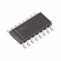
MAX4583ESE+ Maxim Integrated Products, MAX4583ESE+ Datasheet - Page 9

MAX4583ESE+
Manufacturer Part Number
MAX4583ESE+
Description
IC SWITCH TRIPLE SPDT 16SOIC
Manufacturer
Maxim Integrated Products
Datasheet
1.MAX4582LEEE.pdf
(18 pages)
Specifications of MAX4583ESE+
Function
Switch
Circuit
3 x SPDT
On-state Resistance
80 Ohm
Voltage Supply Source
Single, Dual Supply
Voltage - Supply, Single/dual (±)
2 V ~ 12 V, ±2 V ~ 6 V
Current - Supply
1µA
Operating Temperature
-40°C ~ 85°C
Mounting Type
Surface Mount
Package / Case
16-SOIC (0.154", 3.90mm Width)
Number Of Switches
Triple
Switch Configuration
SPDT
On Resistance (max)
80 Ohms
On Time (max)
200 ns
Off Time (max)
100 ns
Off Isolation (typ)
- 74 dB
Supply Voltage (max)
+/- 6 V
Supply Voltage (min)
+/- 2 V
Maximum Power Dissipation
696 mW
Maximum Operating Temperature
+ 85 C
Mounting Style
SMD/SMT
Description/function
Analog Switch
Input Level
CMOS, TTL
Minimum Operating Temperature
- 40 C
Off State Leakage Current (max)
1 nA
Lead Free Status / RoHS Status
Lead free / RoHS Compliant
will conduct. During normal operation, these and other
reverse-biased ESD diodes leak, forming the only cur-
rent drawn from V
Virtually all the analog leakage current comes from the
ESD diodes. Although the ESD diodes on a given sig-
nal pin are identical and therefore fairly well balanced,
they are reverse biased differently. Each is biased by
either V
their leakages will vary as the signal varies. The differ-
ence in the two diode leakages to the V
pins constitutes the analog-signal-path leakage current.
All analog leakage current flows between each pin and
one of the supply terminals, not to the other switch ter-
minal. This is why both sides of a given switch can
Table 1. Truth Table/Switch Programming
X = Don’t care
*C not present on MAX4582.
Note: Input and output pins are identical and interchangeable. Either may be considered an input or output; signals pass equally
ENABLE
INPUT
H
L
L
L
L
L
L
L
L
well in either direction.
CC
or V
EE
C*
H
H
H
H
X
L
L
L
L
CC
_______________________________________________________________________________________
and the analog signal. This means
or V
SELECT INPUTS
EE
.
B
H
H
H
H
X
L
L
L
L
A
H
H
H
H
X
L
L
L
L
CC
and V
Low-Voltage, CMOS Analog
All switches open
EE
MAX4581
X–X0
X–X1
X–X2
X–X3
X–X4
X–X5
X–X6
X–X7
show leakage currents of either the same or opposite
polarity.
There is no connection between the analog-signal
paths and GND.
V
translators, and set the input logic limits. The logic-level
translators convert the logic levels into switched V
and V
nals. This drive signal is the only connection between
the logic supplies and signals and the analog supplies.
V
The logic-level thresholds are TTL/CMOS compatible
when V
CC
CC
Multiplexers/Switches
and V
and GND power the internal logic and logic-level
EE
CC
signals to drive the gates of the analog sig-
EE
is +5V. As V
All switches open
ON SWITCHES
have ESD-protection diodes to GND.
MAX4582
X–X0,
X–X1,
X–X2,
X–X3,
X–X0,
X–X1,
X–X2,
X–X3,
Y–Y0
Y–Y1
Y–Y2
Y–Y3
Y–Y0
Y–Y1
Y–Y2
Y–Y3
CC
rises, the threshold increases
All switches open
MAX4583
X–X0,
Y–Y0,
X–X1,
Y–Y0,
X–X0,
Y–Y1,
X–X1,
Y–Y1,
X–X0,
Y–Y0,
X–X1,
Y–Y0,
X–X0,
Y–Y1,
X–X1,
Y–Y1,
Z–Z0
Z–Z0
Z–Z0
Z–Z0
Z–Z1
Z–Z1
Z–Z1
Z–Z1
CC
9


