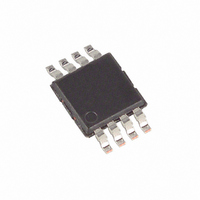
MAX4641EUA+ Maxim Integrated Products, MAX4641EUA+ Datasheet - Page 7

MAX4641EUA+
Manufacturer Part Number
MAX4641EUA+
Description
IC SWITCH DUAL SPST 8UMAX
Manufacturer
Maxim Integrated Products
Datasheet
1.MAX4641EUA.pdf
(10 pages)
Specifications of MAX4641EUA+
Function
Switch
Circuit
2 x SPST - NO
On-state Resistance
4 Ohm
Voltage Supply Source
Single Supply
Voltage - Supply, Single/dual (±)
1.8 V ~ 5.5 V
Current - Supply
1µA
Operating Temperature
-40°C ~ 85°C
Mounting Type
Surface Mount
Package / Case
8-TSSOP, 8-MSOP (0.118", 3.00mm Width)
Number Of Switches
Dual
Switch Configuration
SPDT
On Resistance (max)
4 Ohms
On Time (max)
15 ns
Off Time (max)
8 ns
Off Isolation (typ)
- 80 dB
Supply Voltage (max)
5.5 V
Supply Voltage (min)
1.8 V
Supply Current
0.001 uA
Maximum Power Dissipation
362 mW
Maximum Operating Temperature
+ 85 C
Mounting Style
SMD/SMT
Description/function
Analog Switch
Input Level
CMOS, TTL
Minimum Operating Temperature
- 40 C
Off State Leakage Current (max)
0.25 nA
Lead Free Status / RoHS Status
Lead free / RoHS Compliant
The MAX4641/MAX4642/MAX4643 operate from a sin-
gle supply ranging from +1.8V to +5.5V. The devices
are guaranteed to be functional over that supply range,
but TTL/CMOS compatibility is only valid for operation
using a +5V supply. All voltage levels are referenced to
GND. Positive and negative DC analog inputs or AC
signals can be accommodated by shifting V+ and
GND.
ESD-protection diodes are internally connected be-
tween each analog-signal pin and both V+ and GND.
One of these diodes conducts if any analog signal
Figure 1. Overvoltage Protection Using External Blocking
Diodes
TOP VIEW
NO_, NC_
Pin Configurations/Functional Diagrams/Truth Tables (continued)
Applications Information
COM1
GND
NO1
IN2
High-Speed, Low-Voltage, 4Ω, Dual SPST
_______________________________________________________________________________________
1
2
3
4
IN_
0
1
MAX4641
MAX4641
QFN
GND
V+
NO_
OFF
ON
8
7
6
5
V+
IN1
COM2
NO2
COM
COM1
GND
NC1
IN2
1
2
3
4
IN_
0
1
MAX4642
MAX4642
QFN
CMOS Analog Switches
exceeds V+ or GND (Figure 1). Virtually all of the ana-
log leakage current comes from the ESD diodes to V+
or GND. Although the ESD diodes on a given signal pin
are identical, and therefore fairly well balanced, they
are reverse biased differently. Each is biased by either
V+ or GND and the analog signal. This means their
leakages will vary as the signal varies. The difference in
the two diode leakages to the V+ and GND pins consti-
tutes the analog-signal-path leakage current. All analog
leakage current flows between each pin and one of the
supply terminals, not to the other switch terminal. This
is why both sides of a given switch can show leakage
currents of the same or opposite polarity.
There is no normal current path between the analog-
signal paths and V+ or GND. V+ and GND also power
the internal logic and logic-level translators. The logic-
level translators convert the logic level into switched V+
and GND signals to drive the analog signal gates.
NC_
OFF
ON
8
7
6
5
V+
IN1
COM2
NC2
COM1
GND
NO1
IN2
IN_
0
1
1
2
3
4
MAX4643
MAX4643
QFN
NO1
OFF
ON
8
7
6
5
NC2
OFF
ON
V+
IN1
COM2
NC2
7


