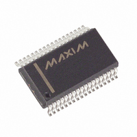
MAX4549EAX+ Maxim Integrated Products, MAX4549EAX+ Datasheet - Page 16

MAX4549EAX+
Manufacturer Part Number
MAX4549EAX+
Description
IC AUD/VIDCROSSPOINT SWIT 36SSOP
Manufacturer
Maxim Integrated Products
Datasheet
1.MAX4549EAX.pdf
(20 pages)
Specifications of MAX4549EAX+
Function
Audio/Video Crosspoint Switch
Circuit
3 x 3:2
On-state Resistance
35 Ohm
Voltage Supply Source
Single Supply
Voltage - Supply, Single/dual (±)
2.7 V ~ 5.5 V
Current - Supply
6µA
Operating Temperature
-40°C ~ 85°C
Mounting Type
Surface Mount
Package / Case
36-BSOP (0.300", 7.5mm Width)
Lead Free Status / RoHS Status
Lead free / RoHS Compliant
Serially Controlled, Triple 3x2 Audio/Video
Crosspoint Switches
The MAX4548 uses an 8-bit slave address. To select a
slave address, connect A0 and A1 to V+ or GND. The
MAX4548 has four possible slave addresses, thus a
maximum of four of these devices may share the same
2-bit address bus. The slave devices on the MAX4548
monitor the serial bus continuously, waiting for a start
condition followed by an address byte. When a slave
device recognizes its address, it acknowledges that it is
ready for further communication by pulling the SDA line
low for one clock period.
The MAX4549 3-wire serial interface is SPI/QSPI/
MICROWIRE-compatible. An active-low chip-select (CS)
input enables the device to receive data for the serial
input (DIN). Data is clocked in on the rising edge of the
serial-clock (SCLK) signal. A total of 24 bits is needed in
each write cycle. Segmented write cycles are allowed
(three 8-bit-wide transfers) if CS remains low. The first
bit clock into the MAX4549 is the command byte’s MSB,
and the last bit clocked in is the data byte’s LSB. When
programming the COM_ _ registers and the Clickless
Mode register, the last eight bits of the data word are
“don’t care.” While shifting data, the device remains in
its original configuration. After all 24 bits are clocked
into the input shift register, a rising edge on CS latches
the data into the MAX4549 internal registers, initiating
the device’s change of state. Figures 6 and 7 and Table
7 show the details of the 3-wire protocol, as it applies to
the MAX4549.
DOUT is the shift register’s output. Data at DOUT is sim-
ply the input data delayed by 24 clock cycles, with data
appearing synchronous with SCLK’s falling edge.
Transitions at DIN and SCLK have no effect when CS is
high, and DOUT holds the last bit in the shift register.
To program several MAX4549s, “daisy-chain” the devices
by connecting DOUT of the first device to DIN of the sec-
ond, and so on. The CS pins of all devices are connected
together, and data is shifted through the MAX4549 in
series. Twenty-four bits of data per device are required
for proper programming of all devices. When CS is
brought high, all devices are updated simultaneously.
To program several MAX4549s individually using a sin-
gle processor, connect the DIN pins of each MAX4549
together and control CS on each MAX4549 separately.
To select a particular device, drive the corresponding
CS low, clock in the 24-bit command, then drive CS high
to execute the command. Typically only one MAX4549
is addressed at a time.
16
______________________________________________________________________________________
Addressable Serial Interface
Slave Address (Address Byte)
3-Wire Serial Interface
Daisy-Chaining
To improve off-isolation, connect the S_ input to ground
either directly (DC ground) or through capacitors (AC
ground). Closing S_ then effectively grounds the unused
outputs.
Use the internal bias-resistor networks to give the
switch outputs a DC bias when the switch terminals are
AC-coupled. Programming the switches that connect
the bias resistors to the inputs is accomplished via bit
C6 of the command byte. Connect _BIASH and _BIASL
inputs to DC levels (for example, V+ and GND), and
activate the switch connecting the appropriate outputs.
This applies a voltage midway between _BIASH and
_BIASL to the input (refer to Tables 1 and 4, and the
Functional Diagram ). To improve crosstalk when using
the bias resistors, connect the MID_ inputs to ground
through capacitors.
Audible switching transients (“clicks”) are eliminated in
this mode of operation. When an output is configured as
“clickless,” the gate signal of the switches connected to
the output are controlled with slow-moving voltages. As
a result, the output slew rates are significantly reduced.
Program clickless operation via bit C7 of the command
byte (refer to Tables 1 and 4, and the Functional
Diagram ). Each operating switch may draw 2mA during
a transition. When another command is given while a
switch is changing state in the soft mode, the
MAX4548/MAX4549 will complete the previous com-
mand in the hard mode. To avoid this situation, do not
issue a second command until the transition of the
switch is complete.
The MAX4548/MAX4549 feature a preset power-up state.
Refer to Tables 2, 3, and 4 to determine the power-up
state of the devices.
The MAX4548/MAX4549 have five bypass pins for the
internal bias resistor networks (MID_). The equivalent AC
impedance at these pins is 10kΩ. To improve crosstalk
performance, bypass MID_ pins with 10µF. For lowest
cost, standard aluminum electrolytic capacitors in parallel
with 0.1µF ceramic chip capacitors perform well in audio
applications. For computer audio applications, a single
1µF capacitor is sufficient. For telecom voice applica-
tions, a 0.1µF capacitor is adequate. For video applica-
tions, bypass MID_ with 0.1µF in parallel with 1000pF.
This provides a low impedance across the entire video
bandwidth.
Using the Internal Bias Resistors
Improving Off-Isolation
Clickless Switching
Bypass Capacitors
Power-Up State


