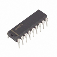
DG528CJ+ Maxim Integrated Products, DG528CJ+ Datasheet - Page 8

DG528CJ+
Manufacturer Part Number
DG528CJ+
Description
IC MULTIPLEXER 8X1 18DIP
Manufacturer
Maxim Integrated Products
Type
Analog Multiplexerr
Datasheet
1.DG529CWN.pdf
(12 pages)
Specifications of DG528CJ+
Function
Multiplexer
Circuit
1 x 8:1
On-state Resistance
400 Ohm
Voltage Supply Source
Single, Dual Supply
Voltage - Supply, Single/dual (±)
5 V ~ 30 V, ±4.5 V ~ 20 V
Operating Temperature
0°C ~ 70°C
Mounting Type
Through Hole
Package / Case
18-DIP (0.300", 7.62mm)
Package
18PDIP N
Maximum On Resistance
450@±15V Ohm
Multiplexer Architecture
8:1
Maximum Turn-on Time
1500@±15V ns
Power Supply Type
Single|Dual
Lead Free Status / RoHS Status
Lead free / RoHS Compliant
8-Channel Latchable Multiplexers
Maxim guarantees the DG528/DG529 for operation
from ±4.5V to ±20V supplies. The switching delays
increase by about a factor of two at ±5V, and break-
before-make action is preserved.
The DG528/DG529 can operate with a single +5V to
+30V supply as well as asymmetrical power supplies
like +15V and -5V. The digital threshold will remain
approximately 1.6V above the GND pin, and the analog
characteristics such as r
total voltage difference between V+ and V-. Connect V-
to 0V when operating with a +5V to +30V single supply.
Figure 8. Simplified Internal Structure
8
_______________________Applications
_______________________________________________________________________________________
EN
A_
WR
RS
PROTECTION
PROTECTION
PROTECTION
PROTECTION
Operation with Supply Voltages
DS(ON)
4-WIDE LATCH
CLK
are determined by the
RESET
Other Than ±15V
LEVEL SHIFT
The typical digital threshold of both the address lines
and EN is 1.6V with a temperature coefficient of
approximately -3mV/°C, ensuring compatibility with TTL
logic over the temperature range. The digital threshold
is relatively independent of the power-supply voltages,
going from a typical 1.6V when V+ is 15V to 1.5V typi-
cal with V+ = 5V. Therefore, Maxim’s DG528/DG529
operate with standard TTL logic levels, even with ±5V
power supplies. In all cases, EN’s threshold is the same
as the other logic inputs and is referenced to GND.
The digital inputs can also be driven with CMOS logic
levels swinging from either V+ to V- or from V+ to GND.
The digital input current is just a few nanoamps of leak-
age at all input-voltage levels with a guaranteed maxi-
mum of 1µA. The digital inputs are protected from ESD
by a 30V zener diode between the input and V+ and
can be driven ±2V beyond the supplies without draw-
ing excessive current.
DECODE
Digital Interface Levels
V+
D
S1
Sn
V-


