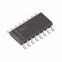
MAX314FESE+ Maxim Integrated Products, MAX314FESE+ Datasheet - Page 10

MAX314FESE+
Manufacturer Part Number
MAX314FESE+
Description
IC SWITCH QUAD SPST 16SOIC
Manufacturer
Maxim Integrated Products
Datasheet
1.MAX314FESE.pdf
(15 pages)
Specifications of MAX314FESE+
Function
Switch
Circuit
4 x SPST - NC/NO
On-state Resistance
10 Ohm
Voltage Supply Source
Single, Dual Supply
Voltage - Supply, Single/dual (±)
4.5 V ~ 30 V, ±4.5 V ~ 20 V
Operating Temperature
-40°C ~ 85°C
Mounting Type
Surface Mount
Package / Case
16-SOIC (0.154", 3.90mm Width)
Lead Free Status / RoHS Status
Lead free / RoHS Compliant
state. If the switch state is off, all FETs are turned off and
both NO_ (or NC_) and COM_ are high impedance.
When the signal on NO_ (or NC_) and COM_ exceeds V-,
the low-fault comparator output is high, turning off FETs
N1 and P1. This makes the NO_ (or NC_) and COM_ pins
high impedance regardless of the switch state. If the
switch state is off, all FETs are turned off and both NO_
(or NC_) and COM_ are high impedance.
When a fast rise-time and fall-time transient on NO_,
NC_, or COM_ exceeds V+ or V-, the output follows the
input to the supply rail with only a few nanoseconds
delay. This delay is due to the switch on-resistance and
circuit capacitance to ground. When the input transient
returns to within the supply rails, however, there is a
longer output recovery time delay. For positive faults,
the recovery time is typically 1µs. For negative faults,
the recovery time is typically 0.6µs. These values
depend on the output resistance and capacitance, and
are not production tested or guaranteed. The delays
are not dependent on the fault amplitude. Higher load
resistance and capacitance increase recovery times.
The maximum fault voltage on the NO_ (or NC_) and
COM_ pins is ±36V with power applied and ±40V with
power off.
Exceeding the fault-protection voltage limits on NO_,
NC_, or COM_, even for very short periods, can cause
the device to fail (see the Absolute Maximum Ratings).
The failure modes may not be obvious, and failure in
one switch may or may not affect other switches in the
same package.
Quad, Rail-to-Rail, Fault-Protected,
SPST Analog Switches
10
Transient Fault Response and Recovery
______________________________________________________________________________________
Fault-Protection Voltage and Power Off
Negative Fault Condition
Failure Modes
There is no galvanic connection between the analog
signal paths and GND. The analog signal paths consist
of an N-channel and P-channel MOSFET with their
sources and drains paralleled and their gates driven
out of phase to V+ and V- by the logic-level translators.
However, the potential of the analog signals must be
defined or at least limited with respect to GND.
V+ and GND power the internal logic and logic-level
translators and set the input logic thresholds. The logic-
level translators convert the logic levels to switched V+
and V- signals to drive the gates of the analog switch-
es. This drive signal is the only connection between the
power supplies and the analog signals.
The MAX312F/MAX313F/MAX314F operate with bipolar
supplies between ±4.5V and ±20V. The V+ and V- sup-
plies need not be symmetrical, but their difference can-
not exceed the absolute maximum rating of 44V.
The MAX312F/MAX313F/MAX314F operate from a sin-
gle supply between +9V and +36V when V- is connect-
ed to GND.
TRANSISTOR COUNT: 251
PROCESS: CMOS
SUBSTRATE CONNECTED TO: V+
MAX313FESE
MAX313FEPE
MAX314FESE
MAX314FEPE
Ordering Information (continued)
PART
-40°C to +85°C
-40°C to +85°C
-40°C to +85°C
-40°C to +85°C
TEMP RANGE
Chip Information
Bipolar Supplies
PIN-PACKAGE
16 SO
16 Plastic DIP
16 SO
16 Plastic DIP
Single Supply
Ground


