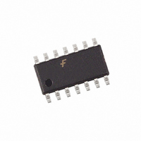
MM74HC4066SJ Fairchild Semiconductor, MM74HC4066SJ Datasheet - Page 2

MM74HC4066SJ
Manufacturer Part Number
MM74HC4066SJ
Description
IC SWITCH 1X1 14SOP
Manufacturer
Fairchild Semiconductor
Series
74HCr
Specifications of MM74HC4066SJ
Function
Switch
Circuit
1 x 1:1
On-state Resistance
70 Ohm
Voltage Supply Source
Single Supply
Voltage - Supply, Single/dual (±)
2 V ~ 12 V
Current - Supply
8µA
Operating Temperature
-40°C ~ 85°C
Mounting Type
Surface Mount
Package / Case
14-SOIC (0.200", 5.30mm Width)
Lead Free Status / RoHS Status
Lead free / RoHS Compliant
Available stocks
Company
Part Number
Manufacturer
Quantity
Price
Company:
Part Number:
MM74HC4066SJ
Manufacturer:
FAIR
Quantity:
2 089
www.fairchildsemi.com
V
V
R
R
I
I
I
I
IN
IZ
IZ
CC
Supply Voltage (V
DC Control Input Voltage (V
DC Switch I/O Voltage (V
Clamp Diode Current (I
DC Output Current, per pin (I
DC V
Storage Temperature Range (T
Power Dissipation (P
Lead Temperature (T
Symbol
Absolute Maximum Ratings
(Note 2)
DC Electrical Characteristics
Note 4: For a power supply of 5V 10% the worst case on resistance (R
this supply. Worst case V
CMOS at the higher voltage and so the 5.5V values should be used.
Note 5: At supply voltages (V
these devices be used to transmit digital only when using these supply voltages.
IH
IL
ON
ON
(Note 3)
S.O. Package only
(Soldering 10 seconds)
CC
or GND Current, per pin (I
Minimum HIGH Level
Input Voltage
Maximum LOW Level
Input Voltage
Maximum “ON” Resistance
(Note 5)
Maximum “ON” Resistance
Matching
Maximum Control
Input Current
Maximum Switch “OFF”
Leakage Current
Maximum Switch “ON”
Leakage Current
Maximum Quiescent
Supply Current
Parameter
CC
IH
)
D
L
)
)
and V
IK
CC
, I
IO
–GND) approaching 2V the analog switch on resistance becomes extremely non-linear. Therefore it is recommended that
OK
IL
)
IN
occur at V
OUT
)
)
STG
)
CC
V
V
(Figure 1)
V
V
(Figure 1)
V
V
V
V
V
V
V
V
V
V
I
)
V
OUT
CTL
IS
CTL
IS
CTL
IS
IN
CC
OS
IS
CTL
IS
CTL
IN
OS
CC
)
V
V
V
V
V
GND or V
V
V
Conditions
2 6V
V
0 A
5.5V and 4.5V respectively. (The V
EE
CC
CC
CC
CC
V
V
V
CC
V
V
OPEN (Figure 2)
CC
CC
IH
IH
IH
IL
IH
or GND
to GND
to GND
or GND
to GND
or GND
, I
, I
(Figure 3)
or GND
1.5 to V
0.5 to V
65 C to 150 C
S
S
(Note 1)
CC
2.0 mA
2.0 mA
0.5 to 15V
(Note 4)
CC
CC
600 mW
500 mW
20 mA
25 mA
50 mA
260 C
ON
1.5V
0.5V
) occurs for HC at 4.5V. Thus the 4.5V values should be used when designing with
12.0V
12.0V
12.0V
12.0V
12.0V
12.0V
12.0V
2.0V
4.5V
9.0V
2.0V
4.5V
9.0V
4.5V
9.0V
12.0
2.0V
4.5V
9.0V
4.5V
9.0V
6.0V
9.0V
6.0V
9.0V
6.0V
9.0V
V
CC
2
Recommended Operating
Conditions
Note 1: Absolute Maximum Ratings are those values beyond which dam-
age to the device may occur.
Note 2: Unless otherwise specified all voltages are referenced to ground.
Note 3: Power Dissipation temperature derating — plastic “N” package:
12 mW/ C from 65 C to 85 C.
Supply Voltage (V
DC Input or Output Voltage
Input Rise or Fall Times
Operating Temperature Range (T
(V
(t
r
, t
IH
IN
Typ
100
120
50
30
50
35
20
10
10
15
20
10
15
20
f
, V
5
5
value at 5.5V is 3.85V.) The worst case leakage current occurs for
) V
T
A
OUT
V
V
CC
CC
CC
25 C
)
3.15
1.35
170
180
1.5
6.3
8.4
0.5
2.7
3.6
2.0
4.0
8.0
2.0V
4.5V
9.0V
85
70
80
60
40
15
10
10
100
0.1
60
80
40
50
60
CC
)
T
A
Guaranteed Limits
40 to 85 C T
3.15
1.35
200
105
215
100
1000
1.5
5.3
8.4
0.5
2.7
3.6
85
75
60
20
15
15
600
800
150
200
300
20
40
80
1.0
A
)
Min
A
2
0
40
55 to 125 C
3.15
1.35
220
110
240
120
1000
160
1.5
6.3
8.4
0.5
2.7
3.6
90
80
70
20
15
15
600
800
150
200
300
40
80
1.0
1000
Max
V
500
400
12
85
CC
Units
ns
ns
ns
V
V
Units
C
nA
nA
nA
nA
nA
nA
V
V
V
V
V
V
V
V
A
A
A
A


