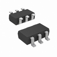
DG447DV-T1-E3 Vishay, DG447DV-T1-E3 Datasheet - Page 7

DG447DV-T1-E3
Manufacturer Part Number
DG447DV-T1-E3
Description
IC SWITCH DUAL SPST 6TSOP
Manufacturer
Vishay
Type
Analog Switchr
Datasheet
1.DG448DV-T1-E3.pdf
(8 pages)
Specifications of DG447DV-T1-E3
Function
Switch
Circuit
2 x SPST - NC
On-state Resistance
25 Ohm
Voltage Supply Source
Single, Dual Supply
Voltage - Supply, Single/dual (±)
7 V ~ 36 V, ± 4.5 V ~ 20 V
Current - Supply
16µA
Operating Temperature
-40°C ~ 85°C
Mounting Type
Surface Mount
Package / Case
6-TSOP (0.063", 1.60mm Width)
Number Of Switches
1
Switch Configuration
SPST
On Resistance (max)
45 Ohms
On Time (max)
175 ns
Off Time (max)
120 ns
Off Isolation (typ)
- 72 dB
Supply Voltage (max)
44 V
Supply Voltage (min)
7 V
Supply Current
0.016 mA
Maximum Power Dissipation
570 mW
Maximum Operating Temperature
+ 85 C
Mounting Style
SMD/SMT
Minimum Operating Temperature
- 40 C
Switch Current (typ)
30 mA
Analogue Switch Type
SPST
No. Of Channels
1
On State Resistance Max
25ohm
Turn Off Time
50ns
Turn On Time
100ns
Supply Voltage Range
± 4.5V To ± 20V
Operating Temperature Range
-40°C To
Package
6TSOP
Maximum On Resistance
45@12V Ohm
Maximum High Level Output Current
30 mA
Maximum Turn-off Time
120@12V ns
Maximum Turn-on Time
175@12V ns
Switch Architecture
SPST
Power Supply Type
Single|Dual
Lead Free Status / RoHS Status
Lead free / RoHS Compliant
Lead Free Status / RoHS Status
Lead free / RoHS Compliant, Lead free / RoHS Compliant
Other names
DG447DV-T1-E3TR
Available stocks
Company
Part Number
Manufacturer
Quantity
Price
Company:
Part Number:
DG447DV-T1-E3
Manufacturer:
Maxim
Quantity:
534
TEST CIRCUITS
V
Vishay Siliconix maintains worldwide manufacturing capability. Products may be manufactured at one of several qualified locations. Reliability data for Silicon
Technology and Package Reliability represent a composite of all qualified locations. For related documents such as package/tape drawings, part marking, and
reliability data, see www.vishay.com/ppg?73854.
Document Number: 73854
S09-1260-Rev. C, 13-Jul-09
V
O
gen
V
is the steady state output with the switch on.
S
R
g
= 50
0V , 2.4 V
3 V
R
g
Ω
Figure 3. Off Isolation
COM
IN
GND
NO/NC
IN
Of f Isolation = 20 log
GND
+ 15 V
NO/NC
- 15 V
0 V 2.4 V
V +
V -
+ 15 V
,
- 15 V
V -
V +
COM
IN
IN
Figure 5. Source/Drain Capacitances
C
V
V
O
S
1 nF
C
GND
C
L
Figure 2. Charge Injection
V
O
R
V
O
L
- 15 V
+ 15 V
V -
V +
NO/NC
COM
V
C
C
C
C
S
R
g
0 V, 2.4 V
= 50
V
Ω
IN
O
or Equivalent
Impedance
HP4192A
X
f = 1 MHz
Analyzer
Meter
Figure 4. Insertion Loss
OFF
NO/NC
IN
GND
DG447, DG448
Q = ΔV
+ 15 V
- 15 V
Vishay Siliconix
ON
V +
V -
COM
O
x C
www.vishay.com
L
C
C
OFF
R
ΔV
L
O
V
O
7


