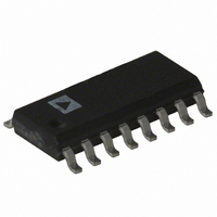
ADG774BR Analog Devices Inc, ADG774BR Datasheet - Page 5

ADG774BR
Manufacturer Part Number
ADG774BR
Description
IC MUX/DEMUX QUAD 2X1 16SOIC
Manufacturer
Analog Devices Inc
Type
Analog Multiplexerr
Datasheet
1.ADG774BRZ.pdf
(12 pages)
Specifications of ADG774BR
Rohs Status
RoHS non-compliant
Function
Multiplexer/Demultiplexer
Circuit
4 x 2:1
On-state Resistance
3.5 Ohm
Voltage Supply Source
Single Supply
Voltage - Supply, Single/dual (±)
1.8 V ~ 5.5 V
Current - Supply
0.001µA
Operating Temperature
-40°C ~ 85°C
Mounting Type
Surface Mount
Package / Case
16-SOIC (0.154", 3.90mm Width)
Package
16SOIC N
Maximum Data Rate
16 Mbps
Maximum On Resistance
9@3V Ohm
Maximum High Level Output Current
100 mA
Multiplexer Architecture
2:1
Maximum Turn-off Time
11@3V@-40C to 125C ns
Maximum Turn-on Time
21@3V@-40C to 125C ns
Power Supply Type
Single
Available stocks
Company
Part Number
Manufacturer
Quantity
Price
Part Number:
ADG774BR
Manufacturer:
ADI/亚德诺
Quantity:
20 000
Part Number:
ADG774BR-REEL7
Manufacturer:
ADI/亚德诺
Quantity:
20 000
Part Number:
ADG774BRQ
Manufacturer:
ADI/亚德诺
Quantity:
20 000
Part Number:
ADG774BRQZ
Manufacturer:
ADI/亚德诺
Quantity:
20 000
Part Number:
ADG774BRQZ-REEL
Manufacturer:
ADI/亚德诺
Quantity:
20 000
REV. C
V
GND
S
D
IN
EN
R
R
I
I
I
V
C
C
C
t
t
t
Crosstalk
Off Isolation
Bandwidth
Distortion
S
D
D
ON
OFF
D
R
DD
ON
FLAT(ON)
D
S
D
D
, I
(OFF)
(OFF)
, C
ON
(OFF)
(V
(OFF)
S
(ON)
S
S
)
(ON)
Ground (0 V) Reference.
Logic Control Input.
Frequency Response of the Switch in the ON State Measured at 3 dB Down.
Most Positive Power Supply Potential.
Source Terminal. May be an input or output.
Drain Terminal. May be an input or output.
Logic Control Input.
Ohmic Resistance between D and S.
On Resistance Match between any Two Channels, i.e., R
Flatness is defined as the difference between the maximum and minimum value of on resistance as measured over
the specified analog signal range.
Source Leakage Current with the Switch OFF.
Drain Leakage Current with the Switch OFF.
Channel Leakage Current with the Switch ON.
Analog Voltage on Terminals D, S.
OFF Switch Source Capacitance.
OFF Switch Drain Capacitance.
ON Switch Capacitance.
Delay between Applying the Digital Control Input and the Output Switching on. See Test Circuit 4.
Delay between Applying the Digital Control Input and the Output Switching Off.
OFF Time or ON Time Measured between the 90% Points of Both Switches, When Switching from One Address
State to Another. See Test Circuit 5.
A Measure of Unwanted Signal that is Coupled through from One Channel to Another as a Result of Parasitic
Capacitance.
A Measure of Unwanted Signal Coupling through an OFF Switch.
R
FLAT(ON)
/R
L
GND
PIN CONFIGURATION
S1A
S1B
S2A
S2B
D1
D2
IN
TERMINOLOGY
(SOIC/QSOP)
1
3
4
5
6
7
8
2
(Not to Scale)
TOP VIEW
ADG774
–5–
16
15
14
13
12
11
10
9
ON
V
EN
S4A
S4B
D4
S3A
S3B
D3
DD
max – R
ON
min.
ADG774


