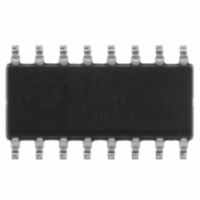
PI5V330SWE Pericom Semiconductor, PI5V330SWE Datasheet - Page 3

PI5V330SWE
Manufacturer Part Number
PI5V330SWE
Description
IC VIDEO MUX/DEMUX 2X1 16SOIC
Manufacturer
Pericom Semiconductor
Datasheet
1.PI5V330SWE.pdf
(8 pages)
Specifications of PI5V330SWE
Function
Video Multiplexer/Demultiplexer
Circuit
4 x 2:1
On-state Resistance
10 Ohm
Voltage Supply Source
Single Supply
Voltage - Supply, Single/dual (±)
4.5 V ~ 5.5 V
Current - Supply
0.1µA
Operating Temperature
-40°C ~ 85°C
Mounting Type
Surface Mount
Package / Case
16-SOIC (0.154", 3.90mm Width)
Number Of Channels
4 Channel
On Resistance (max)
7 Ohms (Typ) @ 5 V
On Time (max)
5 ns @ @ 5 V @ - 40 C to 85 C
Off Time (max)
5 ns @ @ 5 V @ - 40 C to 85 C
Maximum Power Dissipation
500 mW
Maximum Operating Temperature
+ 85 C
Minimum Operating Temperature
- 40 C
Mounting Style
SMD/SMT
Lead Free Status / RoHS Status
Lead free / RoHS Compliant
Available stocks
Company
Part Number
Manufacturer
Quantity
Price
Company:
Part Number:
PI5V330SWEX
Manufacturer:
PERICO
Quantity:
9 300
Notes:
1.
Notes:
1.
2.
3.
4.
Dynamic Characteristics
Power Supply Characteristics
t
t
B
X
C
C
C
O
Parameters
ON
OFF
Parameters
W
IN
OFF
ON
TALK
IRR
For Max. or Min. conditions, use appropriate value specifi ed under Electrical Characteristics for the applicable device.
Typical values are at V
Per TTL driven input (V
This current applies to the control inputs only and represent the current required to switch internal capacitance at the specifi ed frequency. The
S1, S2, and D I/O pins generate no signifi cant AC or DC currents as they transition. This parameter is not tested, but is guar an teed by design.
(1)
This parameter is determined by device characterization but is not production tested.
(1)
I
(1)
∆
I
(1)
CCD
CC
ICC
09-0124
Turn On Time
Turn Off Time
-3 dB Bandwidth
Crosstalk
Input/Enable Capacitance
Capacitance, Switch Off
Capacitance, Switch On
Off Isolation
Quiescent Power
Supply Current
Supply Current per Input
@ TTL HIGH
Supply Current per Input
per MHz
Description
DD
Description
(4)
IN
= 5.0V, +25°C ambient.
= 3.4V, control inputs only); S1, S2, and D pins do not contribute to I
(Over the Operating Range, T
V
V
V
Pins Open EN = GND
Control Input Toggling
50% Duty Cycle
DD
DD
DD
R
R
See Fig. 5
10MHz, See Fig. 5, C
V
V
V
10MHz, See Fig 5, C
L
L
IN
IN
IN
= Max.
= Max.
= Max., S1, S2 and D
= 75Ω, C
= 75Ω, C
= 0V, f = 1 MHz
= 0V, f = 1 MHz
= 0V, f = 1 MHz
L
L
Test Conditions
A
= 20
= 20
= –40°C to +85°C, V
Test Conditions
3
PF
PF
, See Fig. 4
, See Fig. 4
L
L
= 0pF
= 0pF
IN = GND or V
IN = 3.4V
(1)
DD
Low On-Resistance Wideband/Video
(3)
= 5V ±5%)
CC
DD
.
Quad 2-Channel Mux/DeMux
Min.
Min.
Typ
Typ.
-80
-48
2.5
1.1
0.1
(2)
PS7032I
Max.
Max.
0.25
570
3.0
2.5
5
5
6
6
9
PI5V330S
Units
MHz
MHz
mA/
Unit
mA
μA
dB
dB
06/26/09
pF
ns


