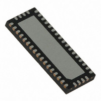
PI2PCIE2412ZHE Pericom Semiconductor, PI2PCIE2412ZHE Datasheet - Page 3

PI2PCIE2412ZHE
Manufacturer Part Number
PI2PCIE2412ZHE
Description
IC MUX/DEMUX 2X1 42VQFN
Manufacturer
Pericom Semiconductor
Type
Analog Multiplexerr
Datasheet
1.PI2PCIE2412ZHE.pdf
(10 pages)
Specifications of PI2PCIE2412ZHE
Function
Multiplexer/Demultiplexer
Circuit
4 x 2:1
Voltage Supply Source
Single Supply
Voltage - Supply, Single/dual (±)
1.5 V ~ 2 V
Current - Supply
200µA
Operating Temperature
-40°C ~ 85°C
Mounting Type
Surface Mount
Package / Case
42-VQFN
Package
42TQFN EP
Maximum Data Rate
5000 Mbps
Maximum High Level Output Current
120 mA
Multiplexer Architecture
2:1
Power Supply Type
Single
Number Of Channels
4 Channel
Off Time (max)
8 ns
Supply Voltage (max)
2 V
Supply Voltage (min)
1.5 V
Maximum Power Dissipation
500 mW
Maximum Operating Temperature
+ 85 C
Minimum Operating Temperature
- 40 C
Mounting Style
SMD/SMT
Supply Voltage Range
1.5V To 2V
Operating Temperature Range
-40°C To +85°C
Digital Ic Case Style
TQFN
No. Of Pins
42
Filter Terminals
SMD
Communication Function
Switch
No. Of Channels
4
Rohs Compliant
Yes
Lead Free Status / RoHS Status
Lead free / RoHS Compliant
Lead Free Status / RoHS Status
Lead free / RoHS Compliant
Available stocks
Company
Part Number
Manufacturer
Quantity
Price
Company:
Part Number:
PI2PCIE2412ZHE
Manufacturer:
PER
Quantity:
2 790
Company:
Part Number:
PI2PCIE2412ZHE
Manufacturer:
Pericom
Quantity:
640
Part Number:
PI2PCIE2412ZHE
Manufacturer:
PERICOM
Quantity:
20 000
Part Number:
PI2PCIE2412ZHEX
Manufacturer:
FERICOM
Quantity:
20 000
Maximum Ratings
(Above which useful life may be impaired. For user guide lines, not tested.)
DC Electrical Characteristics for Switching over Operating Range
Power Supply Characteristics
Switching Characteristics
Dynamic Electrical Characteristics Over the Operating Range
Notes:
1.
2.
I
t PZH , t PZL
t PHZ , t PLZ
t b-b
t ch-ch
V IH
V IL
V IK
I IH
I IL
X
O
I
BW
Parameters
Parameters
Storage Temperature ....................................................–65°C to +150°C
Supply Voltage to Ground Potential ................................–0.5V to +2.5V
DC Input Voltage .............................................................. –0.5V to V
DC Output Current ....................................................................... 120mA
Power Dissipation ........................................................................... 0.5W
CC
LOSS
Parameters
Parameters
TALK
IRR
For Max. or Min. conditions, use appropriate value specifi ed under Electrical Characteristics for the applicable device type.
Typical values are at V
09-0049
Quiescent Power Supply Current
Line Enable Time - SEL to A N , B N, C N
Line Disable Time - SEL to A N , B N, C N
Bit-to-bit skew within the same differential pair
Channel-to-channel skew
Crosstalk
OFF Isolation
Differential
Insertion Loss
Bandwidth -3dB
Input HIGH Voltage
Input LOW Voltage
Clamp Diode Voltage
Input HIGH Current
Input LOW Current
Description
DD
= 1.8V, T
Description
Description
(T A = -40º to +85ºC, V DD = 1.8V±10%)
A
= 25°C ambient and maximum loading.
See Fig. 1 for Measurement Setup, f= 3 GHz
See Fig. 2 for Measurement Setup, f= 3 GHz
f= 3 GHz
Description
Guaranteed HIGH level
Guaranteed LOW level
V
V
V
Test Conditions
DD
DD
DD
V
DD
= Max., I
= Max., V
= Max., V
Test Conditions
= Max., V
3
IN
Test Conditions
IN
IN
= –18mA
DD
= V
= GND
IN
4-Differential Channel, 2:1 Mux/DeMux Switch
f = 100 MHz
f = 100 MHz
= GND or V
DD
(1)
Note: Stresses greater than those listed under MAX I MUM
RAT INGS may cause permanent damage to the de vice. This
is a stress rating only and func tion al op er a tion of the device
at these or any other conditions above those indicated in the
operational sections of this spec i fi ca tion is not implied. Expo-
sure to absolute max i mum rating con di tions for extended
periods may affect re li abil i ty.
(T A = -40º to +85ºC, V DD = 1.8V±10%, GND=0V)
(1)
(T
DD
1.8V, PCI Express Gen2 Compliant,
A
= –40°C to +85°C, V
0.65 x
Min.
Min
V
–0.5
DD
Min.
Typ.
-23dB
-58dB
-23dB
-58dB
Typ
4.1
-2
–0.7
Min.
Typ.
0.5
0.5
(2)
200
(2)
(2)
DD
Max.
PS8866C
Max.
= 1.5V to 2.0V)
PI2PCIE2412
0.35 x
Max.
8.0
8.0
35
Max
V
–1.2
7
±5
±5
DD
Units
Units
GHz
Units
dB
dB
Units
μA
ns
ps
ps
03/11/09
μA
V


