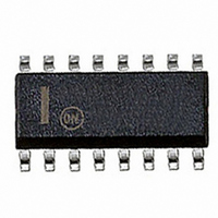
MC74HC4051ADR2G ON Semiconductor, MC74HC4051ADR2G Datasheet - Page 10

MC74HC4051ADR2G
Manufacturer Part Number
MC74HC4051ADR2G
Description
IC MUX/DEMUX 8X1 16SOIC
Manufacturer
ON Semiconductor
Series
74HCr
Type
Analog Multiplexerr
Datasheet
1.MC74HC4053ANG.pdf
(18 pages)
Specifications of MC74HC4051ADR2G
Function
Multiplexer/Demultiplexer
Circuit
1 x 8:1
On-state Resistance
100 Ohm
Voltage Supply Source
Single, Dual Supply
Voltage - Supply, Single/dual (±)
±2 V ~ 6 V, 2 V ~ 12 V
Current - Supply
40µA
Operating Temperature
-55°C ~ 125°C
Mounting Type
Surface Mount
Package / Case
16-SOIC (0.154", 3.90mm Width)
On Resistance (max)
190 Ohms
Propagation Delay Time
40 ns
On Time (max)
245 ns
Off Time (max)
160 ns
Supply Voltage (max)
6 V
Supply Voltage (min)
2 V
Maximum Power Dissipation
500 mW
Maximum Operating Temperature
+ 125 C
Minimum Operating Temperature
- 55 C
Bandwidth
80 MHz
Mounting Style
SMD/SMT
Number Of Switches
Single
Multiplexer Configuration
Single 8:1
Number Of Inputs
8
Number Of Outputs
1
Number Of Channels
1
Analog Switch On Resistance
190@4.5VOhm
Analog Switch Turn On Time
245ns
Analog Switch Turn Off Time
160ns
Package Type
SOIC
Power Supply Requirement
Single/Dual
Single Supply Voltage (min)
2V
Single Supply Voltage (typ)
3/5V
Single Supply Voltage (max)
6V
Dual Supply Voltage (min)
±1V
Dual Supply Voltage (typ)
±3/±5V
Dual Supply Voltage (max)
±6V
Power Dissipation
500mW
Mounting
Surface Mount
Pin Count
16
Operating Temp Range
-55C to 125C
Operating Temperature Classification
Military
Dc
0705
Lead Free Status / RoHS Status
Lead free / RoHS Compliant
Other names
MC74HC4051ADR2GOS
MC74HC4051ADR2GOS
MC74HC4051ADR2GOSTR
MC74HC4051ADR2GOS
MC74HC4051ADR2GOSTR
Available stocks
Company
Part Number
Manufacturer
Quantity
Price
Company:
Part Number:
MC74HC4051ADR2G
Manufacturer:
ON Semiconductor
Quantity:
4
Part Number:
MC74HC4051ADR2G
Manufacturer:
MOT/ON
Quantity:
20 000
V
high and GND being recognized as a logic low. In this
example:
the supply voltages V
voltage should not exceed V
analog voltage should not go below V
the difference between V
using the configuration of Figure 15, a maximum analog
signal of ten volts peak-to-peak can be controlled. Unused
analog inputs/outputs may be left floating (i.e., not
connected). However, tying unused analog inputs and
f
in
f
in
CC
The Channel Select and Enable control pins should be at
The maximum analog voltage swings are determined by
Figure 14a. Total Harmonic Distortion, Test Set-Up
0.1mF
or GND logic levels. V
V
V
EE
0.1mF
EE
Figure 12. Crosstalk Between Any Two
R
L
V
IS
V
R
IS
L
*Includes all probe and jig capacitance
V
6
7
8
GND = 0V = logic low
Switches, Test Set-Up
CC
6
7
8
*Includes all probe and jig capacitance
CC
ON
= +5V = logic high
OFF
ON
and V
CC
CC
V
16
and V
CC
CC
MC74HC4051A, MC74HC4052A, MC74HC4053A
. Similarly, the negative peak
16
EE
being recognized as a logic
. The positive peak analog
EE
R
L
R
is ten volts. Therefore,
L
V
EE
OS
. In this example,
C
L
APPLICATIONS INFORMATION
C
*
L
*
DISTORTION
METER
R
L
TO
http://onsemi.com
V
OS
C
L
*
10
outputs to V
minimize crosstalk and feed-through noise that may be
picked up by an unused switch.
requirement. The only constraints on the power supplies are
that:
anticipated on the analog channels, external Germanium or
Schottky diodes (D
16. These diodes should be able to absorb the maximum
anticipated current surges during clipping.
- 100
- 10
- 20
- 30
- 40
- 50
- 60
- 70
- 80
- 90
Although used here, balanced supplies are not a
When voltage transients above V
0
Figure 13. Power Dissipation Capacitance,
1.0
Figure 14b. Plot, Harmonic Distortion
CC
ANALOG I/O
FUNDAMENTAL FREQUENCY
V
EE
or GND through a low value resistor helps
V
V
V
EE
CC
CC
x
V
) are recommended as shown in Figure
CC
- GND = 0 to -6 volts
and V
- GND = 2 to 6 volts
- V
Test Set-Up
FREQUENCY (kHz)
EE
CHANNEL SELECT
6
7
8
EE
ON/OFF
OFF/ON
= 2 to 12 volts
2.0
≤ GND
CC
V
16
11
CC
DEVICE
SOURCE
and/or below V
COMMON O/I
A
V
CC
EE
NC
3.125
are


