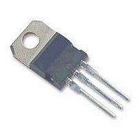
AUIRL3705N International Rectifier, AUIRL3705N Datasheet - Page 2

AUIRL3705N
Manufacturer Part Number
AUIRL3705N
Description
54T9027
Manufacturer
International Rectifier
Datasheet
1.AUIRL3705N.pdf
(11 pages)
Specifications of AUIRL3705N
Transistor Polarity
N Channel
Continuous Drain Current Id
89A
Drain Source Voltage Vds
55V
On Resistance Rds(on)
0.01ohm
Rds(on) Test Voltage Vgs
10V
Power Dissipation Pd
170W
Rohs Compliant
Yes
Configuration
Single
Resistance Drain-source Rds (on)
10 mOhms
Drain-source Breakdown Voltage
55 V
Gate-source Breakdown Voltage
+/- 16 V
Continuous Drain Current
89 A
Power Dissipation
170 W
Mounting Style
Through Hole
Package / Case
TO-220AB
Gate Charge Qg
65.3 nC
Minimum Operating Temperature
- 55 C
Lead Free Status / Rohs Status
Details
Available stocks
Company
Part Number
Manufacturer
Quantity
Price
Company:
Part Number:
AUIRL3705N
Manufacturer:
IR
Quantity:
12 500
V
∆V
R
V
gfs
I
I
Q
Q
Q
t
t
t
t
L
L
C
C
C
I
I
V
t
Q
t
Static Electrical Characteristics @ T
Dynamic Electrical Characteristics @ T
Diode Characteristics
Notes:
Repetitive rating; pulse width limited by max. junction temperature. (See fig. 11).
‚
ƒ I
„
… Calculated continuous current based on maximum allowable junction temperature. for
DSS
GSS
d(on)
r
d(off)
f
S
SM
rr
on
D
S
(BR)DSS
DS(on)
GS(th)
iss
oss
rss
SD
g
gs
gd
rr
2
(BR)DSS
recommended current-handling of the package refer to Design tip # 93-4
SD
≤
/∆T
J
≤
Drain-to-Source Breakdown Voltage
Breakdown Voltage Temp. Coefficient
Static Drain-to-Source On-Resistance
Gate Threshold Voltage
Forward Transconductance
Drain-to-Source Leakage Current
Gate-to-Source Forward Leakage
Gate-to-Source Reverse Leakage
Total Gate Charge
Gate-to-Source Charge
Gate-to-Drain ("Miller") Charge
Turn-On Delay Time
Rise Time
Turn-Off Delay Time
Fall Time
Internal Drain Inductance
Internal Source Inductance
Input Capacitance
Output Capacitance
Reverse Transfer Capacitance
Continuous Source Current
(Body Diode)
Pulsed Source Current
(Body Diode)
Diode Forward Voltage
Reverse Recovery Time
Reverse Recovery Charge
Forward Turn-On Time
≤
Parameter
Parameter
™
≤
≤
J
≤
= 25°C (unless otherwise specified)
J
Ω
= 25°C (unless otherwise specified)
Intrinsic turn-on time is negligible (turn-on is dominated by LS+LD)
Min.
Min.
–––
–––
–––
–––
–––
–––
–––
–––
–––
–––
–––
–––
–––
–––
–––
–––
–––
–––
–––
–––
–––
–––
–––
–––
–––
1.0
55
50
0.056
Typ.
Typ.
3600
–––
–––
–––
–––
–––
–––
–––
–––
–––
–––
–––
–––
–––
140
870
320
–––
–––
–––
290
4.5
7.5
12
37
78
94
Max. Units
0.010
0.012
0.018
Max. Units
-100
89
–––
–––
–––
250
100
–––
–––
–––
–––
–––
–––
–––
–––
–––
310
140
440
2.0
1.3
25
98
19
49
g
V/°C
µA
nA
nC
nH
nC
ns
pF
ns
V
Ω
V
S
A
V
V
Reference to 25°C, I
V
V
V
V
V
V
V
V
V
I
V
V
V
I
R
R
Between lead,
6mm (0.25in.)
from package
and center of die contact
V
V
ƒ = 1.0MHz, See Fig.5
MOSFET symbol
showing the
integral reverse
p-n junction diode.
T
T
di/dt = 100A/µs
D
D
J
J
GS
GS
GS
GS
DS
DS
DS
DS
GS
GS
DS
GS
DD
G
D
GS
DS
= 46A
= 46A
= 25°C, I
= 25°C, I
= 0.59Ω, See Fig.10
= 1.8Ω,V
= V
= 25V, I
=55V, V
= 44V, V
= 44V
= 25V
= 0V, I
= 10V, I
= 5.0V, I
= 4.0V, I
= 16V
= -16V
= 5.0V,See Fig 6 and 13
= 28V
= 0V
GS
, I
D
D
S
F
D
D
GS
GS
= 250µA
D
D
GS
= 250µA
= 46A
= 46A
= 46A, V
= 46A
= 46A
= 39A
= 5.0V
= 0V
= 0V, T
f
Conditions
Conditions
g
D
f
f
f
= 1mA
GS
J
= 150°C
f
= 0V
G
f
www.irf.com
G
f
D
S
S
D


