ADM00360 Microchip Technology, ADM00360 Datasheet - Page 12
ADM00360
Manufacturer Part Number
ADM00360
Description
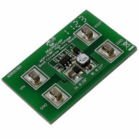
Power Management Modules & Development Tools MCP16301 300mA D2PAK Footprint Demo Board
Manufacturer
Microchip Technology
Series
-r
Datasheet
1.ADM00360.pdf
(18 pages)
Specifications of ADM00360
Featured Product
MCP16301 Demo Boards
Main Purpose
DC/DC, Step Down
Outputs And Type
1, Non-Isolated
Power - Output
-
Voltage - Output
3.3V
Current - Output
300mA
Voltage - Input
4 ~ 26 V
Regulator Topology
Buck
Frequency - Switching
500kHz
Board Type
Fully Populated
Utilized Ic / Part
MCP16301
Lead Free Status / Rohs Status
Details


MCP16301 300 mA D
2.2
DS51983A-page 12
GETTING STARTED
The MCP16301 300 mA D
and demonstrate the MCP16301 capability.
2.2.1
2.2.1.1
The MCP16301 300 mA D
evaluation. Apply positive input voltage to the V
return to the GND terminal. The maximum input voltage should not exceed 26V. An
electronic load or resistive load can be used for evaluation or the intended system load
can be connected. The electronic loads attempt to sink current at 0V during startup. A
resistive load or constant resistance is recommended for startup evaluation. Connect
the positive voltage terminal of the load to the V
connect the negative or return side of the load to the GND terminal.
2.2.1.2
To test the board, follow the next steps:
1. Apply the input voltage.
2. An internal pull up resistor is connected from V
3. The measured output voltage should be 3.3V typical. Adjusting the input voltage
2.2.2
The MCP16301 integrates a low resistance N-Channel MOSFET. A high side or
floating supply is needed to drive the gate of the N-Channel MOSFET above the input
voltage to turn it on. The demo board uses the output voltage (3.3V) to charge the boost
cap, while inductor current flows, clamping the SW node to a diode drop below ground.
Prior to start up, there is no inductor current, so an internal pre-charge circuit charges
the boost cap up to a minimum threshold. Once charged, the N-Channel can be turned
on, ramping current into the inductor.
The worst case operating conditions for charging the boost capacitor occur at minimum
V
the boost cap to a high value. At no load, the converter is operating at a minimum or
very low duty cycle, putting a small amount of current into the inductor. When the switch
turns off the inductor, current decays very quickly, resulting in a small time to recharge
the boost capacitor.
IN
and no load. At minimum V
MCP16301. Once the input voltage is greater than 3.5V, the device begins to
switch. Apply greater than 4V supply to the input for proper operation. A minimum
load is required to regulate the output to 3.3V. For minimum load requirements
(light load conditions), detailed information is provided in the data sheet.
and load should not cause the output to vary more than a few mV over the oper-
ating range of the converter.
Power Input and Output Connection
POWERING THE MCP16301 300 MA D
BOARD TESTING
How the MCP16301 300 mA D
Operates
2
PAK Demo Board User’s Guide
2
2
PAK Demo Board is fully assembled and tested to evaluate
PAK Demo Board is fully assembled, tested and ready for
IN
(4V), there is not enough head room to pre-charge
2
PAK Demo Board Boost Strap
IN
OUT
terminal and the corresponding
IN
2
PAK DEMO BOARD
terminal on the demo board, and
to the EN input of the
© 2011 Microchip Technology Inc.
Related parts for ADM00360
Image
Part Number
Description
Manufacturer
Datasheet
Request
R

Part Number:
Description:
Manufacturer:
Microchip Technology Inc.
Datasheet:
Part Number:
Description:
Manufacturer:
Microchip Technology Inc.
Datasheet:
Part Number:
Description:
Manufacturer:
Microchip Technology Inc.
Datasheet:
Part Number:
Description:
Manufacturer:
Microchip Technology Inc.
Datasheet:
Part Number:
Description:
Manufacturer:
Microchip Technology Inc.
Datasheet:
Part Number:
Description:
Manufacturer:
Microchip Technology Inc.
Datasheet:
Part Number:
Description:
Manufacturer:
Microchip Technology Inc.
Datasheet:
Part Number:
Description:
Manufacturer:
Microchip Technology Inc.
Datasheet: