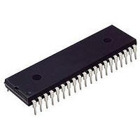
HD3-6402R-9 Intersil, HD3-6402R-9 Datasheet - Page 6

HD3-6402R-9
Manufacturer Part Number
HD3-6402R-9
Description
06F5779
Manufacturer
Intersil
Datasheet
1.HD3-6402R-9Z.pdf
(7 pages)
Specifications of HD3-6402R-9
No. Of Channels
8
Uart Features
Programmable Word Length, Stop Bits And Parity, Automatic Data Formatting And Status Generation
Supply Voltage Range
4.5V To 5.5V
Rohs Compliant
No
Available stocks
Company
Part Number
Manufacturer
Quantity
Price
Company:
Part Number:
HD3-6402R-9
Manufacturer:
N/A
Quantity:
5 704
Company:
Part Number:
HD3-6402R-9
Manufacturer:
N/A
Quantity:
5 704
Part Number:
HD3-6402R-9
Manufacturer:
HAR
Quantity:
20 000
Absolute Maximum Ratings
Supply Voltage . . . . . . . . . . . . . . . . . . . . . . . . . . . . . . . . . . . . . +8.0V
Input, Output or I/O Voltage Applied . . . . . GND -0.5V to V
Storage Temperature Range . . . . . . . . . . . . . . . . . -65
Junction Temperature . . . . . . . . . . . . . . . . . . . . . . . . . . . . . .+175
Lead Temperature (Soldering 10s) . . . . . . . . . . . . . . . . . . . .+300
ESD Classification . . . . . . . . . . . . . . . . . . . . . . . . . . . . . . . . . Class 1
Typical Derating Factor . . . . . . . . . . . 1mA/MHz Increase in ICCOP
CAUTION: Stresses above those listed in “Absolute Maximum Ratings” may cause permanent damage to the device. This is a stress only rating and operation of the
device at these or any other conditions above those indicated in the operational sections of this specification is not implied.
Operating Conditions
Operating Voltage Range. . . . . . . . . . . . . . . . . . . . . . +4.5V to +5.5V
Capacitance
AC Electrical Specifications
DC Electrical Specifications
NOTE: Guaranteed, but not 100% tested
Input Capacitance
Output Capacitance
(1) fCLOCK
(2) t
(3) t
(4) t
(5) t
(6) t
SYMBOL
SYMBOL
ICCOP
ICCSB
PW
MR
SET
HOLD
EN
V
V
V
V
I
OH
II
OL
O
IH
IL
PARAMETER
Logical ‘‘1’’ Input Voltage
Logical ‘‘0’’ Input Voltage
Input Leakage Current
Logical ‘‘1’’ Output Voltage
Logical ‘‘0’’ Output Voltage
Output Leakage Current
Standby Supply Current
Operating Supply Current (See Note)
T
A
Clock Frequency
Pulse Widths, CRL, DRR, TBRL
Pulse Width MR
Input Data Setup Time
Input Data Hold Time
Output Enable Time
= +25
o
C
PARAMETER
PARAMETER
6
V
V
CC
CC
= 5.0V ± 10%, T
= 5.0V ± 10%, T
SYMBOL
COUT
CIN
o
C to +150
Freq. = 1MHz, all measurements are referenced to device
GND
CC
LIMITS HD-6402R
A
A
D.C.
MIN
150
150
V CC -0.4
50
60
+0.5V
= -40
= -40
-
MIN
-1.0
-1.0
2.0
3.0
o
o
o
-
-
-
-
HD-6402
HD-6402
C
C
C
o
o
C to +85
C to +85
LIMITS
MAX
160
2.0
-
-
-
-
o
o
MAX
Thermal Information
Thermal Resistance (Typical)
Gate Count . . . . . . . . . . . . . . . . . . . . . . . . . . . . . . . . . . .1643 Gates
*Pb-free PDIPs can be used for through hole wave solder processing
only. They are not intended for use in Reflow solder processing
applications.
Operating Temperature Range
100
C (HD3-6402R-9)
C (HD3-6402R-9)
0.8
1.0
0.4
1.0
2.0
-
-
-
CONDITIONS
CERDIP Package. . . . . . . . . . . . . . . .
PDIP Package*. . . . . . . . . . . . . . . . . .
HD3-6402R-9 . . . . . . . . . . . . . . . . . . . . . . . . . . . . -40
LIMITS HD-6402B
D.C.
MIN
150
75
20
20
-
UNITS
mA
µA
µA
µA
V
V
V
V
MAX
8.0
35
-
-
-
-
V
V
V
I
I
I
V
V
Output Open
V
V
OH
OH
OL
CC
CC
IN
O
IN
CC
IN
UNITS
MHz
= GND or V
= +2.5mA, V
= GND or V
= GND or V
= V
= -2.5mA, V
= -100µA
ns
ns
ns
ns
ns
= 5.5V
= 4.5V
= 5.5V, Clock Freq. = 2MHz,
CC
or GND, Outputs Open
C
See Switching Waveform
CONDITIONS
L
CC
CC
CC
= 50pF
CC
CC
TYPICAL
, V
, V
; V
50
50
LIMIT
= 4.5V
= 4.5V
CONDITIONS
25
25
CC
θ
CC
CC
o
o
JA
C/W
C/W
= 5.5V
= 5.5V
= 5.5V,
o
C to +85
12
UNITS
N/A
θ
pF
pF
o
JC
C/W
o
C


