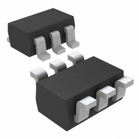
MAX4707EXT+T Maxim Integrated Products, MAX4707EXT+T Datasheet - Page 6

MAX4707EXT+T
Manufacturer Part Number
MAX4707EXT+T
Description
IC SWITCH SPST SC70-6
Manufacturer
Maxim Integrated Products
Datasheet
1.MAX4706EXKT.pdf
(11 pages)
Specifications of MAX4707EXT+T
Function
Switch
Circuit
1 x SPST- NO
On-state Resistance
3 Ohm
Voltage Supply Source
Single Supply
Voltage - Supply, Single/dual (±)
1.8 V ~ 5.5 V
Current - Supply
1µA
Operating Temperature
-40°C ~ 85°C
Mounting Type
Surface Mount
Package / Case
6-TSSOP, SC-88, SOT-363
Lead Free Status / RoHS Status
Lead free / RoHS Compliant
The MAX4706/MAX4707 SPST switches operate from a
single supply ranging from 1.8V to 5.5V. The MAX4706
is a normally closed (NC) switch and the MAX4707 is
the normally open (NO) version. These switches provide
3.5Ω on-resistance (R
+2.7V supply. These devices typically consume only
0.02µA of quiescent current, making them suitable for
use in low-power, portable applications. The
MAX4706/MAX4707 feature low-leakage currents over
Low-Voltage, 2Ω, SPST,
CMOS Analog Switches
Figure 1. Overvoltage Protection Using Two External Blocking
Diodes
Figure 2. Switching Time
6
_______________________________________________________________________________________
SWITCH
INPUT
V
LOGIC
INPUT
g
MAX4706
MAX4707
V
COM
COM
C
V
L
OUT
INCLUDES FIXTURE AND STRAY CAPACITANCE.
COM
IN
POSITIVE SUPPLY
= V
GND
ON
COM
Detailed Description
) and 0.9Ω R
(
R
GND
V+
L
D1
D2
R
+ R
L
ON
)
V+
V+
OR NC
N0
NO
MAX4706
MAX4707
ON
flatness with a
R
L
SWITCH
OUTPUT
C
V
L
OUT
the entire temperature range, TTL/CMOS-compatible
digital logic, and excellent AC characteristics.
The MAX4706/MAX4707 are offered in small 5-pin and
6-pin SC70 and 6-pin µDFN packages.
The MAX4706/MAX4707 operate from a single +1.8V to
+5.5V supply. The MAX4706/MAX4707 accept bipolar
input signals when V+ and GND are biased from bipolar
supplies. For example, the switch accepts a 1V
when V+ = 2V and GND = -2V. ESD-protection diodes
are internally connected between each analog switch
terminal and both V+ and GND. One of these diodes
conducts if any analog signal is greater than V+ or less
than GND (Figure 1). Virtually all analog leakage current
is attributed to the ESD diodes. Each diode is biased by
the analog signal and either V+ or GND. The ESD
diodes’ leakage currents vary as the signal changes.
Caution: Do not exceed the absolute maximum
ratings because stresses beyond the listed ratings
may cause permanent damage to the device.
Proper power-supply sequencing is recommended for
all CMOS devices. Always apply V+ before applying
analog signals, especially if the analog signal is not
current-limited.
SWITCH
OUTPUT
LOGIC
INPUT
V
OUT
LOGIC INPUT WAVEFORMS INVERTED FOR SWITCHES
THAT HAVE THE OPPOSITE LOGIC SENSE.
V+
0V
0V
Applications Information
Power-Supply Sequencing and
t
ON
50%
Overvoltage Protection
0.9 x V
0UT
t
OFF
t r < 5ns
t f < 5ns
0.9 x V
0UT
P-P
input


