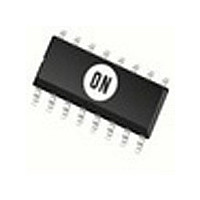
DAC-08ED ON Semiconductor, DAC-08ED Datasheet - Page 2

DAC-08ED
Manufacturer Part Number
DAC-08ED
Description
Manufacturer
ON Semiconductor
Datasheet
1.DAC-08ED.pdf
(14 pages)
Specifications of DAC-08ED
Number Of Channels
1
Resolution
8b
Interface Type
Parallel
Single Supply Voltage (typ)
Not RequiredV
Dual Supply Voltage (typ)
±15V
Settling Time
0.135us
Architecture
Current Steering
Power Supply Requirement
Dual
Output Type
Current
Integral Nonlinearity Error
±0.19LSB
Single Supply Voltage (min)
Not RequiredV
Single Supply Voltage (max)
Not RequiredV
Dual Supply Voltage (min)
±4.5V
Dual Supply Voltage (max)
±18V
Operating Temp Range
0C to 70C
Operating Temperature Classification
Commercial
Mounting
Surface Mount
Pin Count
16
Package Type
SOIC
Lead Free Status / Rohs Status
Not Compliant
Available stocks
Company
Part Number
Manufacturer
Quantity
Price
Part Number:
DAC-08ED
Manufacturer:
S
Quantity:
20 000
Part Number:
DAC-08ED.
Manufacturer:
MOTOROLA/摩托罗拉
Quantity:
20 000
Part Number:
DAC-08EDC
Manufacturer:
RAYTHEON
Quantity:
20 000
Company:
Part Number:
DAC-08EDG
Manufacturer:
BB
Quantity:
5 510
Maximum ratings are those values beyond which device damage can occur. Maximum ratings applied to the device are individual stress limit values
(not normal operating conditions) and are not valid simultaneously. If these limits are exceeded, device functional operation is not implied, damage
may occur and reliability may be affected.
1. Derate above 25°C, at the following rates:
PIN FUNCTION DESCRIPTION
MAXIMUM RATINGS
Power Supply Voltage
Digital Input Voltage
Logic Threshold Control
Applied Output Voltage
Reference Current
Reference Amplifier Inputs
Maximum Power Dissipation
T
Thermal Resistance, Junction−to−Ambient
Lead Soldering Temperature (10 sec max)
Operating Temperature Range
Operating Junction Temperature
Storage Temperature Range
amb
Pin # N Package / D Package
= 25°C (Still-Air) (Note 1)
10/14
11/15
12/16
6/10
8/12
9/13
13/1
14/2
15/3
16/4
7/11
1/5
2/6
3/7
4/8
5/9
V
V
REF
REF
Rating
(+)
(−)
REFERENCE
AMPLIFIER
14
15
13
16
COMP.
V+
+
−
BIAS
NETWORK
CURRENT
SWITCHES
V
1
LC
N Package
D Package
N Package
D Package
V−
COMPEN
Symbol
5
3
N package at 13.3 mW/°C
D package at 9.5 mW/°C.
V
V
MSB
B
V
REF+
REF−
1
V−
B
B
B
B
B
B
B
B
V+
I
I
LC
O
O
1
2
3
4
5
6
7
8
Figure 1. Block Diagram
6
DAC−08 SERIES
B
http://onsemi.com
2
7
B
3
2
8
V+ to V−
V
Symbol
V
T
B
Logic Control Voltage
Inverted Output Current
Negative Power Supply
Non−Inverted Output Current
Output 1, Most Significant Bit (MSB)
Output 2
Output 3
Output 4
Output 5
Output 6
Output 7
Output 8, Least Significant Bit (LSB)
Positive Power Supply
Positive Reference Voltage
Negative Reference Voltage
Compensator Capacitor Pin
14
R
T
5
V
4
SOLD
T
P
V
I
−V
amb
T
14
qJA
stg
, V
LC
D
0
J
12
15
9
B
5
10
B
6
11
B
7
V− to V− plus 36 V
12
LSB
B
−65 to +150
V
Description
8
V− to +18
V− to V+
EE
0 to +70
Value
1450
1090
105
230
150
5.0
36
75
to V
CC
4
2
I
I
OUT
OUT
°C/W
Unit
mW
mA
°C
°C
°C
°C
V
V
−
−
−


