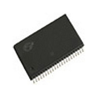
CY62126DV30LL-55ZI Cypress Semiconductor Corp, CY62126DV30LL-55ZI Datasheet

CY62126DV30LL-55ZI
Specifications of CY62126DV30LL-55ZI
Available stocks
Related parts for CY62126DV30LL-55ZI
CY62126DV30LL-55ZI Summary of contents
Page 1
... A 0 Note: 1. For best-practice recommendations, please refer to the Cypress application note “System Design Guidelines” on http://www.cypress.com. Cypress Semiconductor Corporation Document #: 38-05230 Rev. *H 1-Mbit (64K x 16) Static RAM advanced circuit design to provide ultra-low active current. This is ideal for providing More Battery Life™ (MoBL portable applications such as cellular telephones ...
Page 2
... Product Portfolio V Product Range Min. CY62126DV30L Automotive 2.2 CY62126DV30LL Industrial [3, 4] Pin Configurations 48-ball VFBGA Top View BLE I/O BHE I/O I I/O I DNU NC I I Notes: 2. Typical values are included for reference only and are not guaranteed or tested. Typical values are measured ...
Page 3
Maximum Ratings (Above which the useful life may be impaired. For user guide- lines, not tested.) Storage Temperature ................................. –65°C to +150°C Ambient Temperature with Power Applied............................................. –55°C to +125°C Supply Voltage to Ground Potential ..............................................................−0.3 to 3.9V DC Voltage ...
Page 4
Capacitance Parameter Description C Input Capacitance IN C Output Capacitance OUT [8] Thermal Resistance Parameter Description Θ Thermal Resistance (Junction to Ambient) Still Air, soldered 4.5 inch, JA Θ Thermal Resistance (Junction to Case) JC ...
Page 5
Switching Characteristics (Over the Operating Range) Parameter Read Cycle t Read Cycle Time RC t Address to Data Valid AA t Data Hold from Address Change OHA t CE LOW to Data Valid ACE t OE LOW to Data Valid ...
Page 6
Switching Waveforms Read Cycle No. 1 (Address Transition Controlled) ADDRESS DATA OUT PREVIOUS DATA VALID [15, 16] Read Cycle No. 2 (OE Controlled) ADDRESS CE t ACE BHE/BLE LZOE LZOE t DBE t LZBE HIGH IMPEDANCE DATA ...
Page 7
Switching Waveforms (continued) [12, 13, 16, 17, 18] Write Cycle No. 1 (WE Controlled ADDRESS BHE/BLE OE DATA I/O NOTE 19 t HZOE [12, 13, 16, 17, 18] Write Cycle No. 2 (CE Controlled) ADDRESS CE ...
Page 8
Switching Waveforms (continued) Write Cycle No. 3 (WE Controlled, OE LOW) ADDRESS CE BHE/BLE DATAI/O NOTE 19 t HZWE Write Cycle No. 4 (BHE/BLE-controlled, OE LOW) ADDRESS CE BHE/BLE DATA I/O NOTE 19 Document ...
Page 9
... Ordering Information Speed Ordering Code (ns) 55 CY62126DV30LL-55BVI CY62126DV30LL-55BVXI CY62126DV30LL-55ZI CY62126DV30LL-55ZXI CY62126DV30L-55BVXE CY62126DV30L-55ZSXE Please contact your local Cypress sales representative for availability of these parts Document #: 38-05230 Rev. *H Inputs/Outputs High Z Deselect/Power-Down High Z Output Disabled Data Out (I/O –I/O ) Read 0 15 High Z (I/O –I/O ) ...
Page 10
Package Diagrams TOP VIEW A1 CORNER 6.00±0.10 SEATING PLANE C Document #: 38-05230 Rev. *H 48-ball VFBGA ( mm) (51-85150) ...
Page 11
... Document #: 38-05230 Rev. *H © Cypress Semiconductor Corporation, 2006. The information contained herein is subject to change without notice. Cypress Semiconductor Corporation assumes no responsibility for the use of any circuitry other than circuitry embodied in a Cypress product. Nor does it convey or imply any license under patent or other rights. Cypress products are not warranted nor intended to be used for medical, life support, life saving, critical control or safety applications, unless pursuant to an express written agreement with Cypress ...
Page 12
... Added Automotive Specs for I and Page# 4 Changed the address of Cypress Semiconductor Corporation on Page #1 from “3901 North First Street” to “198 Champion Court” Removed 45 ns and 70ns Speed bin from Product offering Removed 56-pin QFN package Updated Ordering Information Table CY62126DV30 MoBL ...


