CY2308SI-5H Cypress Semiconductor Corp, CY2308SI-5H Datasheet - Page 2
CY2308SI-5H
Manufacturer Part Number
CY2308SI-5H
Description
Manufacturer
Cypress Semiconductor Corp
Type
Zero Delay PLL Clock Driverr
Datasheet
1.CY2308SI-5H.pdf
(15 pages)
Specifications of CY2308SI-5H
Number Of Elements
1
Supply Current
70mA
Operating Supply Voltage (typ)
3.3V
Operating Temp Range
-40C to 85C
Package Type
SOIC
Output Frequency Range
10 to 133.3MHz
Operating Supply Voltage (min)
3V
Operating Supply Voltage (max)
3.6V
Operating Temperature Classification
Industrial
Pin Count
16
Lead Free Status / Rohs Status
Not Compliant


Pinouts
Table 1. Pin Definitions - 16 Pin SOIC
Select Input Decoding
Document Number: 38-07146 Rev. *H
Notes
1. Weak pull down.
2. Weak pull down on all outputs.
3. Weak pull ups on these inputs.
4. Outputs inverted on 2308–2 and 2308–3 in bypass mode, S2 = 1 and S1 = 0.
Pin
S2
10
12
13
14
15
16
11
1
2
3
4
5
6
7
8
9
0
0
1
1
REF
CLKA1
CLKA2
V
GND
CLKB1
CLKB2
S2
S1
CLKB3
CLKB4
GND
V
CLKA3
CLKA4
FBK
DD
DD
[3]
[3]
[1]
S1
0
1
0
1
[2]
[2]
[2]
[2]
[2]
[2]
[2]
[2]
Signal
CLOCK A1–A4
Tri-State
Driven
Driven
Driven
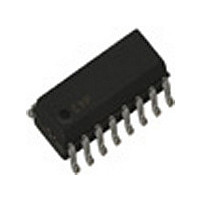
Figure 1. Pin Diagram - 16 Pin SOIC (Top view)
Input reference frequency, 5V tolerant input
Clock output, Bank A
Clock output, Bank A
3.3V supply
Ground
Clock output, Bank B
Clock output, Bank B
Select input, bit 2
Select input, bit 1
Clock output, Bank B
Clock output, Bank B
Ground
3.3V supply
Clock output, Bank A
Clock output, Bank A
PLL feedback input
[4]
CLKA1
CLKA2
CLKB1
CLKB2
GND
REF
V
S2
DD
CLOCK B1–B4
1
2
3
4
5
6
7
8
Driven
Tri-State
Tri-State
Driven
[4]
15
14
13
12
11
10
16
9
FBK
CLKA4
CLKA3
V
GND
CLKB4
CLKB3
S1
DD
Description
Output Source
Reference
PLL
PLL
PLL
PLL Shutdown
Y
N
Y
N
CY2308
Page 2 of 15
[+] Feedback
Related parts for CY2308SI-5H
Image
Part Number
Description
Manufacturer
Datasheet
Request
R

Part Number:
Description:
Manufacturer:
Cypress Semiconductor Corp
Datasheet:
Part Number:
Description:
Manufacturer:
Cypress Semiconductor Corp
Datasheet:
Part Number:
Description:
Manufacturer:
Cypress Semiconductor Corp
Datasheet:
Part Number:
Description:
Manufacturer:
Cypress Semiconductor Corp
Datasheet:
Part Number:
Description:
Manufacturer:
Cypress Semiconductor Corp
Datasheet: