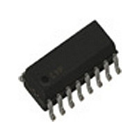
CY2309NZSI-1H Cypress Semiconductor Corp, CY2309NZSI-1H Datasheet - Page 2
CY2309NZSI-1H
Manufacturer Part Number
CY2309NZSI-1H
Description
Manufacturer
Cypress Semiconductor Corp
Datasheet
1.CY2309NZSI-1H.pdf
(6 pages)
Specifications of CY2309NZSI-1H
Number Of Outputs
9
Operating Supply Voltage (max)
3.6V
Operating Temp Range
-40C to 85C
Propagation Delay Time
9.2ns
Operating Supply Voltage (min)
3V
Mounting
Surface Mount
Pin Count
16
Operating Supply Voltage (typ)
3.3V
Package Type
SOIC
Quiescent Current
32uA
Input Frequency
133.33MHz
Duty Cycle
60%
Operating Temperature Classification
Industrial
Lead Free Status / Rohs Status
Not Compliant


Pinouts
Table 1. Pin Description for CY2309NZ
Maximum Ratings
Supply Voltage to Ground Potential................–0.5V to +7.0V
DC Input Voltage (Except REF) ............ –0.5V to V
DC Input Voltage REF .........................................–0.5V to 7V
Operating Conditions
Electrical Characteristics
Document #: 38-07182 Rev. *E
Notes
4, 8, 13
5, 9, 12
1
2, 3, 6, 7, 10,
11, 14, 15, 16
V
T
C
C
BUF_IN, OUTPUT [1:9] Operating Frequency
t
V
V
I
I
V
V
I
PU
IL
IH
DD
1. BUF_IN input has a threshold voltage of V
2. Parameter is guaranteed by design and characterization. It is not 100% tested in production.
Parameter
A
DD
IL
IH
OL
OH
L
IN
Pin
Parameter
Input LOW Voltage
Input HIGH Voltage
Input LOW Current
Input HIGH Current
Output LOW Voltage
Output HIGH Voltage
Supply Current
V
GND
BUF_IN
OUTPUT [1:9]
DD
Description
Supply Voltage
(Ambient Operating Temperature) Commercial
(Ambient Operating Temperature) Industrial
Load Capacitance, Fout < 100 MHz
Load Capacitance,100 MHz < Fout < 133.33 MHz
Input Capacitance
Power up time for all VDDs to reach minimum specified
voltage (power ramps must be monotonic)
Signal
for Commercial and Industrial Temperature Devices
[1]
[1]
[2]
[2]
DD
for Commercial and Industrial Temperature Devices
/2.
3.3V Digital Voltage Supply
Ground
Input Clock
Outputs
Figure 1. CY2309NZ - 16 SOIC-Top View
OUTPUT1
OUTPUT2
OUTPUT3
OUTPUT4
V
V
I
I
Unloaded outputs at 66.66 MHz
OL
OH
Description
IN
IN
BUF_IN
DD
= 8 mA
= 0V
= V
= –8 mA
GND
V
V
DD
DD
+ 0.5V
DD
Test Conditions
1
2
3
4
5
6
7
8
Storage Temperature ................................. –65
Junction Temperature ................................................. 150
Static Discharge Voltage
(per MIL-STD-883, Method 3015) ............................ >2,000V
15
14
13
12
11
10
16
9
OUTPUT9
OUTPUT8
OUTPUT7
V
GND
OUTPUT6
OUTPUT5
GND
DD
Description
0.05
Min
Min
–40
DC
2.0
2.4
3.0
0
133.33
100.0
Max
Max
50.0
3.6
0.8
0.4
70
85
30
15
50
32
7
CY2309NZ
°
C to +150
MHz
Unit
Unit
mA
ms
μA
μA
°
°
pF
pF
pF
V
V
V
V
V
C
C
Page 2 of 6
°
°
C
C
[+] Feedback
Related parts for CY2309NZSI-1H
Image
Part Number
Description
Manufacturer
Datasheet
Request
R

Part Number:
Description:
Manufacturer:
Cypress Semiconductor Corp
Datasheet:
Part Number:
Description:
Manufacturer:
Cypress Semiconductor Corp
Datasheet:
Part Number:
Description:
Manufacturer:
Cypress Semiconductor Corp
Datasheet:
Part Number:
Description:
Manufacturer:
Cypress Semiconductor Corp
Datasheet:
Part Number:
Description:
Manufacturer:
Cypress Semiconductor Corp
Datasheet: