CY62146VLL-70ZI Cypress Semiconductor Corp, CY62146VLL-70ZI Datasheet
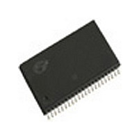
CY62146VLL-70ZI

Manufacturer Part Number
CY62146VLL-70ZI
Description
Manufacturer
Cypress Semiconductor Corp
Datasheet

Specifications of CY62146VLL-70ZI

Density
4Mb
Access Time (max)
70ns
Sync/async
Asynchronous
Architecture
Not Required
Clock Freq (max)
Not RequiredMHz
Operating Supply Voltage (typ)
3V
Address Bus
18b
Package Type
TSOP-II
Operating Temp Range
-40C to 85C
Number Of Ports
1
Supply Current
15mA
Operating Supply Voltage (min)
2.7V
Operating Supply Voltage (max)
3.6V
Operating Temperature Classification
Industrial
Mounting
Surface Mount
Pin Count
44
Word Size
16b
Number Of Words
256K
Lead Free Status / Rohs Status
Not Compliant

Available stocks

Company
Part Number
Manufacturer
Quantity
Price
Part Number:
CY62146VLL-70ZI
Manufacturer:
CYPRESS
Quantity:
14
Part Number:
CY62146VLL-70ZIT
Manufacturer:
LATTICE
Quantity:
5
Cypress Semiconductor Corporation
Document #: 38-05159 Rev. *A
Features
Functional Description
The CY62146V is a high-performance CMOS static RAM
organized as 256K words by 16 bits. These devices feature
advanced circuit design to provide ultra-low active current.
This is ideal for providing More Battery Life
portable applications such as cellular telephones. The device
also has an automatic power-down feature that significantly
reduces power consumption by 99% when addresses are not
toggling. The device can also be put into standby mode when
Note:
• Wide voltage range: 2.7V–3.6V
• Ultra-low active, standby power
• Easy memory expansion with CE and OE features
• TTL-compatible inputs and outputs
• Automatic power-down when deselected
• CMOS for optimum speed/power
• Package available in a standard 44-Pin TSOP Type II
Logic Block Diagram
1.
(forward pinout) package
For best practice recommendations, please refer to the Cypress application note “System Design Guidelines” on http://www.cypress.com.
A
A
A
A
A
A
A
A
A
A
A
10
[1]
4
3
2
1
0
9
8
7
6
5
COLUMN DECODER
®
3901 North First Street
DATA IN DRIVERS
(MoBL
RAM Array
2048 × 2048
256K × 16
®
) in
deselected (CE HIGH). The input/output pins (I/O
I/O
(CE HIGH), outputs are disabled (OE HIGH), BHE and BLE
are disabled (BHE, BLE HIGH), or during a write operation (CE
LOW, and WE LOW).
Writing to the device is accomplished by taking Chip Enable
(CE) and Write Enable (WE) inputs LOW. If Byte Low Enable
(BLE) is LOW, then data from I/O pins (I/O
written into the location specified on the address pins (A
through A
from I/O pins (I/O
specified on the address pins (A
Reading from the device is accomplished by taking Chip
Enable (CE) and Output Enable (OE) LOW while forcing the
Write Enable (WE) HIGH. If Byte Low Enable (BLE) is LOW,
then data from the memory location specified by the address
pins will appear on I/O
LOW, then data from memory will appear on I/O
the truth table at the back of this data sheet for a complete
description of read and write modes.
15
) are placed in a high-impedance state when: deselected
4M (256K x 16) Static RAM
16
San Jose
). If Byte High Enable (BHE) is LOW, then data
8
through I/O
0
to I/O
I/O
I/O
0
8
CA 95134
– I/O
– I/O
7
BHE
WE
CE
OE
BLE
. If Byte High Enable (BHE) is
15
CY62146V MoBL
0
) is written into the location
7
15
through A
Revised August 27, 2002
0
17
through I/O
).
408-943-2600
8
to I/O
0
through
15
. See
7
), is
®
0
[+] Feedback

Related parts for CY62146VLL-70ZI

CY62146VLL-70ZI Summary of contents

Page 1

... A 0 Note: 1. For best practice recommendations, please refer to the Cypress application note “System Design Guidelines” on http://www.cypress.com. Cypress Semiconductor Corporation Document #: 38-05159 Rev (256K x 16) Static RAM deselected (CE HIGH). The input/output pins (I/O I/O ) are placed in a high-impedance state when: deselected ...

Page 2

... VCC + 0.5V Product Portfolio V Range (V) CC Product V V CC(min.) CC(typ.) CY62146VLL 2.7 3.0 Notes –2.0V for pulse durations less than 20 ns. IL(min.) 3. Typical values are included for reference only and are not guaranteed or tested. Typical values are measured at V Document #: 38-05159 Rev. *A ...

Page 3

Electrical Characteristics Over the Operating Range Parameter Description V Output HIGH Voltage OH V Output LOW Voltage OL V Input HIGH Voltage IH V Input LOW Voltage IL I Input Load Current IX I Output Leakage Current ...

Page 4

Parameter Data Retention Characteristics Parameter Description V V for Data Retention Data Retention Current CCDR [4] t Chip Deselect to Data CDR Retention Time [5] t Operation Recovery Time R Data ...

Page 5

Switching Characteristics Over the Operating Range (continued) Parameter t CE LOW to Write End SCE t Address Set-up to Write End AW t Address Hold from Write End HA t Address Set-up to Write Start Pulse Width ...

Page 6

Switching Waveforms (continued) [9, 14, 15] Write Cycle No. 1 (WE Controlled) ADDRESS BHE/BLE OE DATA I/O NOTE 16 t HZOE [9, 14, 15] Write Cycle No. 2 (CE Controlled) ADDRESS CE BHE/BLE WE DATA I/O ...

Page 7

Switching Waveforms (continued) Write Cycle No. 3 (WE Controlled, OE LOW) ADDRESS CE BHE/BLE DATA I/O NOTE 16 t HZWE Write Cycle No. 4 (BHE/BLE Controlled, OE LOW) ADDRESS CE BHE/BLE DATA I/O NOTE ...

Page 8

Typical DC and AC Characteristics Normalized Operating Current vs. Supply Voltage 1.4 1.2 1.0 0.8 0.6 0.4 0.2 0.0 2.7 3.2 SUPPLY VOLTAGE (V) Access Time vs. Supply Voltage 2.7 2.8 SUPPLY ...

Page 9

... Ordering Information Speed (ns) Ordering Code 70 CY62146VLL-70ZI Package Diagram MoBL is a registered trademark, and More Battery Life is a trademark, of Cypress Semiconductor. All product and company names mentioned in this document are the trademarks of their respective holders. Document #: 38-05159 Rev. *A © Cypress Semiconductor Corporation, 2002. The information contained herein is subject to change without notice. Cypress Semiconductor Corporation assumes no responsibility for the use of any circuitry other than circuitry embodied in a Cypress Semiconductor product ...

Page 10

Document Title: CY62146V MoBL 4M (256K x 16) Static RAM Document Number: 38-05159 REV. ECN NO. Issue Date ** 109963 10/02/01 *A 116594 09/04/02 Document #: 38-05159 Rev. *A Orig. of Change Description of Change SZV Change from Spec ...

Related keywords