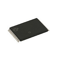
CY62256VL-70ZI Cypress Semiconductor Corp, CY62256VL-70ZI Datasheet - Page 2

CY62256VL-70ZI
Manufacturer Part Number
CY62256VL-70ZI
Description
Manufacturer
Cypress Semiconductor Corp
Datasheet
1.CY62256VL-70ZI.pdf
(12 pages)
Specifications of CY62256VL-70ZI
Density
256Kb
Access Time (max)
70ns
Sync/async
Asynchronous
Architecture
Not Required
Clock Freq (max)
Not RequiredMHz
Operating Supply Voltage (typ)
3V
Address Bus
15b
Package Type
TSOP-I
Operating Temp Range
-40C to 85C
Number Of Ports
1
Supply Current
30mA
Operating Supply Voltage (min)
2.7V
Operating Supply Voltage (max)
3.6V
Operating Temperature Classification
Industrial
Mounting
Surface Mount
Pin Count
28
Word Size
8b
Number Of Words
32K
Lead Free Status / Rohs Status
Not Compliant
Document #: 38-05057 Rev. *F
Product Portfolio
Pin Configurations
Pin Definitions
1–10, 21, 23–26
11–13, 15–19
27
20
22
14
28
Note:
CY62256VLL
2. Typical values are included for reference only and are not guaranteed or tested. Typical values are measured at V
Product
GND
Pin Number
I/O 0
I/O 1
I/O 2
A 10
A 11
A 12
A 13
A 14
A 5
A 6
A 7
A 8
A 9
Narrow SOIC
Top View
13
14
1
2
3
4
5
6
7
8
9
10
11
12
28
27
26
25
24
23
22
21
20
19
18
17
16
15
Com’l/Ind’l
Automotive
Range
V CC
WE
A 4
A 3
A 2
A 1
OE
A 0
CE
I/O 7
I/O 6
I/O 5
I/O 4
I/O 3
Input
Input/Output
Input/Control
Input/Control
Input/Control
Ground
Power Supply
Type
V
Min.
A
A
WE
OE
2.7
A
A
A
A
CC
A
A
A
A
A
11
10
9
8
7
6
5
4
3
2
1
V
CC
26
25
24
23
22
7
6
5
4
3
2
1
28
27
A
I/O
WE. When selected LOW, a WRITE is conducted. When selected HIGH, a READ
is conducted
CE. When LOW, selects the chip. When HIGH, deselects the chip
OE. Output Enable. Controls the direction of the I/O pins. When LOW, the I/O pins
behave as outputs. When deasserted HIGH, I/O pins are Tri-stated, and act as
input data pins
GND. Ground for the device
V
Typ.
Range (V)
CC
0
–A
3.0
0
–I/O
. Power supply for the device
Reverse Pinout
(not to scale)
14
[2]
. Address Inputs
Top View
7
TSOP I
. Data lines. Used as input or output lines depending on operation
Max.
3.6
Speed
(ns)
10
11
12
13
14
15
16
17
18
19
20
21
70
8
9
A
A
A
I/O
I/O
I/O
GND
I/O
I/O
I/O
I/O
I/O
CE
A
12
13
14
0
0
1
2
3
4
5
6
7
V
Operating, I
WE
A
A
OE
CC
Description
Typ.
A
A
A
A
A
A
A
A
A
10
11
1
2
3
4
5
6
7
8
9
11
[2]
22
23
24
25
26
4
5
6
7
27
28
1
2
3
Power Dissipation
CC
CC
(not to scale)
Max.
= V
(mA)
30
Top View
TSOP I
CC(typ.)
, T
A
Standby, I
Typ.
= 25°C, and t
0.1
CY62256V
[2]
21
20
19
18
17
16
15
14
13
12
11
10
9
8
Page 2 of 12
SB2
A
CE
I/O
I/O
I/O
I/O
I/O
GND
I/O
I/O
I/O
A
A
A
AA
0
14
13
12
7
6
5
4
3
2
1
0
Max.
= 70 ns.
130
(µA)
5


