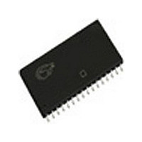
CY7C1019CV33-15ZC Cypress Semiconductor Corp, CY7C1019CV33-15ZC Datasheet - Page 3

CY7C1019CV33-15ZC
Manufacturer Part Number
CY7C1019CV33-15ZC
Description
Manufacturer
Cypress Semiconductor Corp
Datasheet
1.CY7C1019CV33-15ZC.pdf
(10 pages)
Specifications of CY7C1019CV33-15ZC
Density
1Mb
Access Time (max)
15ns
Sync/async
Asynchronous
Architecture
Not Required
Clock Freq (max)
Not RequiredMHz
Operating Supply Voltage (typ)
3.3V
Address Bus
17b
Package Type
TSOP-II
Operating Temp Range
0C to 70C
Number Of Ports
1
Supply Current
70mA
Operating Supply Voltage (min)
2.97V
Operating Supply Voltage (max)
3.63V
Operating Temperature Classification
Commercial
Mounting
Surface Mount
Pin Count
32
Word Size
8b
Number Of Words
128K
Lead Free Status / Rohs Status
Not Compliant
Document #: 38-05130 Rev. *F
Maximum Ratings
(Above which the useful life may be impaired. For user guide-
lines, not tested.)
Storage Temperature ................................. –65°C to +150°C
Ambient Temperature with
Power Applied............................................. –55°C to +125°C
Supply Voltage on V
DC Voltage Applied to Outputs
in High-Z State
DC Input Voltage
Electrical Characteristics
Capacitance
Parameter
V
V
V
V
I
I
I
I
I
C
C
Notes:
IX
OZ
CC
SB1
SB2
2. V
3. Tested initially and after any design or process changes that may affect these parameters.
OH
OL
IH
IL
IN
OUT
IL
(min.) = –2.0V for pulse durations of less than 20 ns.
Parameter
Output HIGH Voltage V
Output LOW Voltage
Input HIGH Voltage
Input LOW Voltage
Input Leakage Current GND < V
Output Leakage
Current
V
Supply Current
Automatic CE
Power-down Current
—TTL Inputs
Automatic CE
Power-down Current
—CMOS Inputs
CC
[2]
[3]
[2]
....................................–0.5V to V
Operating
Description
.................................–0.5V to V
CC
to Relative GND
Input Capacitance
Output Capacitance
[2]
Description
Over the Operating Range
I
V
I
GND < V
Output Disabled
V
I
f = f
Max. V
V
V
Max. V
CE > V
V
or V
OH
OL
OUT
CC
CC
CC
IN
IN
IN
Test Conditions
= 8.0 mA
MAX
[2]
= –4.0 mA
> V
< V
> V
IN
= Min.,
= Min.,
= Max.,
= 0 mA,
.... –0.5V to +4.6V
< 0.3V, f = 0
CC
CC
CC
IH
IL
CC
= 1/t
, f = f
I
I
, CE > V
,
or
< V
< V
– 0.3V,
– 0.3V,
RC
CC
CC
MAX
CC
CC
,
+ 0.5V
+ 0.5V
IH
T
V
A
CC
= 25°C, f = 1 MHz,
Min.
–0.3
= 5.0V
2.4
2.0
–1
–1
Test Conditions
Current into Outputs (LOW)......................................... 20 mA
Static Discharge Voltage............................................ >2001V
(per MIL-STD-883, Method 3015)
Latch-up Current...................................................... >200 mA
Operating Range
–10
Commercial
Industrial
V
CC
Max.
Range
0.4
0.8
+1
+1
80
15
5
+ 0.3
Min.
–0.3
2.4
2.0
–1
–1
–12
V
–40°C to +85°C
Temperature
0°C to +70°C
CC
Max.
0.4
0.8
+1
+1
75
15
Ambient
5
+ 0.3
Max.
CY7C1019CV33
8
8
Min.
–0.3
2.4
2.0
–1
–1
–15
V
CC
Max.
0.4
0.8
+1
+1
70
15
3.3V ± 10%
3.3V ± 10%
5
+ 0.3
Page 3 of 10
Unit
V
pF
pF
CC
Unit
mA
mA
mA
µA
µA
V
V
V
V
[+] Feedback


