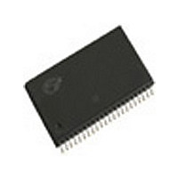
CY7C1021B-12ZC Cypress Semiconductor Corp, CY7C1021B-12ZC Datasheet - Page 4

CY7C1021B-12ZC
Manufacturer Part Number
CY7C1021B-12ZC
Description
Manufacturer
Cypress Semiconductor Corp
Datasheet
1.CY7C1021B-12ZC.pdf
(10 pages)
Specifications of CY7C1021B-12ZC
Density
1Mb
Access Time (max)
12ns
Sync/async
Asynchronous
Architecture
Not Required
Clock Freq (max)
Not RequiredMHz
Operating Supply Voltage (typ)
5V
Address Bus
16b
Package Type
TSOP-II
Operating Temp Range
0C to 70C
Number Of Ports
1
Supply Current
140mA
Operating Supply Voltage (min)
4.5V
Operating Supply Voltage (max)
5.5V
Operating Temperature Classification
Commercial
Mounting
Surface Mount
Pin Count
44
Word Size
16b
Number Of Words
64K
Lead Free Status / Rohs Status
Not Compliant
Available stocks
Company
Part Number
Manufacturer
Quantity
Price
Part Number:
CY7C1021B-12ZC
Manufacturer:
CYP
Quantity:
20 000
Company:
Part Number:
CY7C1021B-12ZCT
Manufacturer:
CY12
Quantity:
3 499
Part Number:
CY7C1021B-12ZCT
Manufacturer:
CYPREE
Quantity:
20 000
Document #: 38-05145 Rev. *C
AC Test Loads and Waveforms
Switching Characteristics
OUTPUT
OUTPUT
Read Cycle
t
t
t
t
t
t
t
t
t
t
t
t
t
t
Write Cycle
t
t
t
t
t
t
t
t
t
t
Notes:
RC
AA
OHA
ACE
DOE
LZOE
HZOE
LZCE
HZCE
PU
PD
DBE
LZBE
HZBE
WC
SCE
AW
HA
SA
SD
HD
LZWE
HZWE
BW
5. Test conditions assume signal transition time of 3 ns or less, timing reference levels of 1.5V, input pulse levels of 0 to 3.0V, and output loading of the specified
6. At any given temperature and voltage condition, t
7. t
8. The internal write time of the memory is defined by the overlap of CE LOW, WE LOW and BHE/BLE LOW. CE, WE and BHE/BLE must be LOW to initiate a write, and
Equivalent to: THÉVENIN
Equivalent to: THÉVENIN
I
the transition of these signals can terminate the write. The input data set-up and hold timing should be referenced to the leading edge of the signal that terminates the write.
INCLUDING
INCLUDING
JIG AND
JIG AND
SCOPE
SCOPE
OL
HZOE
Parameter
/I
5V
5V
OH
, t
and 30-pF load capacitance.
HZBE
30 pF
30 pF
, t
[8]
HZCE
(a)
(a)
EQUIVALENT
EQUIVALENT
, and t
R 481Ω
R 481Ω
Read Cycle Time
Address to Data Valid
Data Hold from Address Change
CE LOW to Data Valid
OE LOW to Data Valid
OE LOW to Low Z
OE HIGH to High Z
CE LOW to Low Z
CE HIGH to High Z
CE LOW to Power-Up
CE HIGH to Power-Down
Byte Enable to Data Valid
Byte Enable to Low Z
Byte Disable to High Z
Write Cycle Time
CE LOW to Write End
Address Set-Up to Write End
Address Hold from Write End
Address Set-Up to Write Start
Data Set-Up to Write End
Data Hold from Write End
WE HIGH to Low Z
WE LOW to High Z
Byte Enable to End of Write
HZWE
are specified with a load capacitance of 5 pF as in part (b) of AC Test Loads. Transition is measured ±500 mV from steady-state voltage.
255Ω
255Ω
OUTPUT
OUTPUT
R2
R2
Over the Operating Range
OUTPUT
OUTPUT
Description
INCLUDING
INCLUDING
JIG AND
JIG AND
SCOPE
SCOPE
[6]
[6]
[6, 7]
[6]
[6, 7]
[6, 7]
5V
5V
HZCE
is less than t
30 pF
30 pF
167
167
5 pF
5 pF
(b)
(b)
LZCE
R 481Ω
, t
HZOE
1.73V
1.73V
[5]
is less than t
255Ω
255Ω
R2
R2
GND
GND
3.0V
3.0V
LZOE
Rise Time: 1 V/ns
Rise Time: 1 V/ns
Min.
12
12
3
0
3
0
0
9
8
0
0
6
0
3
8
7C1021B-12
, and t
HZWE
is less than t
Max.
12
12
12
6
6
6
6
6
6
10%
10%
90%
90%
LZWE
ALL INPUT PULSES
ALL INPUT PULSES
Min.
for any given device.
15
15
10
10
3
0
3
0
0
0
0
8
0
3
9
7C1021B-15
CY7C1021B
Max.
15
15
15
7
7
7
7
7
7
Page 4 of 10
Fall Time: 1 V/ns
90%
90%
10%
10%
Unit
ns
ns
ns
ns
ns
ns
ns
ns
ns
ns
ns
ns
ns
ns
ns
ns
ns
ns
ns
ns
ns
ns
ns
ns
[+] Feedback


