CY7C1021BV33L-15ZI Cypress Semiconductor Corp, CY7C1021BV33L-15ZI Datasheet
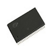
CY7C1021BV33L-15ZI

Manufacturer Part Number
CY7C1021BV33L-15ZI
Description
Manufacturer
Cypress Semiconductor Corp
Datasheet

Specifications of CY7C1021BV33L-15ZI

Density
1Mb
Access Time (max)
15ns
Sync/async
Asynchronous
Architecture
Not Required
Clock Freq (max)
Not RequiredMHz
Operating Supply Voltage (typ)
3.3V
Address Bus
16b
Package Type
TSOP-II
Operating Temp Range
-40C to 85C
Number Of Ports
1
Supply Current
160mA
Operating Supply Voltage (min)
2.97V
Operating Supply Voltage (max)
3.63V
Operating Temperature Classification
Industrial
Mounting
Surface Mount
Pin Count
44
Word Size
16b
Number Of Words
64K
Lead Free Status / Rohs Status
Not Compliant
021BV33
Cypress Semiconductor Corporation
Document #: 38-05148 Rev. *A
Features
Functional Description
The CY7C1021BV is a high-performance CMOS static RAM
organized as 65,536 words by 16 bits. This device has an au-
tomatic power-down feature that significantly reduces power
consumption when deselected.
Selection Guide
Maximum Access Time (ns)
Maximum Operating Current (mA)
Maximum CMOS Standby Current
(mA)
Shaded areas contain advance information.
Note:
Logic Block Diagram
• 3.3V operation (3.0V–3.6V)
• High speed
• CMOS for optimum speed/power
• Low Active Power (L version)
• Low CMOS Standby Power (L version)
• Automatic power-down when deselected
• Independent control of upper and lower bits
• Available in 44-pin TSOP II and 400-mil SOJ
• Available in a 48-Ball Mini BGA package
1.
A
A
A
A
A
A
A
A
— t
— 576 mW (max.)
— 1.80 mW (max.)
1
5
4
3
2
0
7
6
For guidelines on SRAM system design, please refer to the ‘System Design Guidelines’ Cypress application note, available on the internet at www.cypress.com.
AA
= 10/12/15 ns
DATA IN DRIVERS
COLUMN DECODER
512 X 2048
RAM Array
64K x 16
[1]
Commercial
Industrial
Commercial
3901 North First Street
L
7C1021BV-8
0.500
Writing to the device is accomplished by taking Chip Enable
(CE) and Write Enable (WE) inputs LOW. If Byte Low Enable
(BLE) is LOW, then data from I/O pins (I/O
written into the location specified on the address pins (A
through A
from I/O pins (I/O
specified on the address pins (A
Reading from the device is accomplished by taking Chip En-
able (CE) and Output Enable (OE) LOW while forcing the Write
Enable (WE) HIGH. If Byte Low Enable (BLE) is LOW, then
data from the memory location specified by the address pins
will appear on I/O
then data from memory will appear on I/O
truth table at the back of this data sheet for a complete descrip-
tion of read and write modes.
The input/output pins (I/O
high-impedance state when the device is deselected
(CE HIGH), the outputs are disabled (OE HIGH), the BHE and
BLE are disabled (BHE, BLE HIGH), or during a write opera-
tion (CE LOW, and WE LOW).
The CY7C1021BV is available in 400-mil-wide SOJ, standard
44-pin TSOP Type II, and 48-ball mini BGA packages.
170
190
8
5
I/O
I/O
15
1
9
San Jose
BHE
WE
CE
OE
BLE
7C1021BV-10
). If Byte High Enable (BHE) is LOW, then data
–I/O
–I/O
0.500
8
16
160
180
1
10
9
5
to I/O
through I/O
64K x 16 Static RAM
8
I/O 1
I/O 2
I/O 3
I/O 4
V
I/O 5
I/O 6
I/O 7
I/O 8
V
Pin Configurations
WE
A 15
A 14
A 13
A 12
NC
CE
. If Byte High Enable (BHE) is LOW,
CC
A
A 3
A 2
A 1
A 0
SS
1
4
CA 95134
7C1021BV-12
through I/O
SOJ / TSOP II
13
14
15
16
17
18
19
20
21
22
1
2
3
4
5
6
7
8
9
10
11
12
16
Top View
Revised September 13, 2002
CY7C1021BV33
0
0.500
) is written into the location
through A
150
170
12
5
44
43
42
41
40
39
38
37
36
35
34
33
32
31
30
29
28
27
26
25
24
23
16
9
A 5
A 6
A 7
OE
BHE
BLE
I/O 16
I/O 15
I/O 14
I/O 13
V
V
I/O 12
I/O 11
I/O 10
I/O 9
NC
A 8
A 9
A 10
A 11
NC
) are placed in a
1
15
SS
CC
to I/O
through I/O
7C1021BV-15
).
408-943-2600
0.500
16 .
140
160
15
5
See the
8
), is
0
[+] Feedback

Related parts for CY7C1021BV33L-15ZI

CY7C1021BV33L-15ZI Summary of contents

Page 1

... Note: 1. For guidelines on SRAM system design, please refer to the ‘System Design Guidelines’ Cypress application note, available on the internet at www.cypress.com. Cypress Semiconductor Corporation Document #: 38-05148 Rev. *A Writing to the device is accomplished by taking Chip Enable (CE) and Write Enable (WE) inputs LOW. If Byte Low Enable ...

Page 2

Pin Configurations Maximum Ratings (Above which the useful life may be impaired. For user guide- lines, not tested.) Storage Temperature ................................. –65°C to +150°C Ambient Temperature with Power Applied............................................. –55°C to +125°C [2] Supply Voltage Relative GND ...

Page 3

Electrical Characteristics Over the Operating Range Parameter Description Test Conditions V Output HIGH V = Min Voltage I = –4 Output LOW V = Min Voltage V Input HIGH IH Voltage V ...

Page 4

Switching Characteristics Over the Operating Range Parameter Description READ CYCLE t Read Cycle Time RC t Address to Data Valid AA t Data Hold from Address Change OHA t CE LOW to Data Valid ACE t OE LOW to ...

Page 5

Data Retention Waveform Switching Waveforms [11, 12] Read Cycle No. 1 ADDRESS DATA OUT PREVIOUS DATA VALID [12, 13] Read Cycle No. 2 (OE Controlled) ADDRESS CE t ACE OE t DOE BHE, BLE t LZOE t ...

Page 6

Switching Waveforms (continued) [14, 15] Write Cycle No. 1 (CE Controlled) ADDRESS BHE, BLE DATA I/O Write Cycle No. 2 (BLE or BHE Controlled) ADDRESS t SA BHE, BLE WE CE DATA I/O Notes: 14. Data ...

Page 7

Switching Waveforms (continued) Write Cycle No. 3 (WE Controlled, LOW) ADDRESS BHE, BLE DATA I/O Truth Table BLE BHE I High Data ...

Page 8

... CY7C1021BV33-12BAI CY7C1021BV33-12VI 15 CY7C1021BV33-15BAC CY7C1021BV33L-15BAC CY7C1021BV33-15VC CY7C1021BV33L-15VC CY7C1021BV33-15ZC CY7C1021BV33L-15VC CY7C1021BV33-15BAI CY7C1021BV33L-15BAI CY7C1021BV33-15VI CY7C1021BV33L-15ZI Shaded areas contain advance information. Document #: 38-05148 Rev. *A Package Name Package Type BA48A 48-Ball Mini Ball Grid Array (7. 7.00 mm) V34 44-Lead (400-Mil) Molded SOJ V34 44-Lead (400-Mil) Molded SOJ ...

Page 9

Package Diagrams 48-Ball (7. 7. 1.2 mm) FBGA BA48A Document #: 38-05148 Rev. *A CY7C1021BV33 51-85096-*E Page [+] Feedback ...

Page 10

... Document #: 38-05148 Rev. *A © Cypress Semiconductor Corporation, 2002. The information contained herein is subject to change without notice. Cypress Semiconductor Corporation assumes no responsibility for the use of any circuitry other than circuitry embodied in a Cypress Semiconductor product. Nor does it convey or imply any license under patent or other rights. Cypress Semiconductor does not authorize its products for use as critical components in life-support systems where a malfunction or failure may reasonably be expected to result in significant injury to the user ...

Page 11

Document History Page Document Title: CY7C1021BV33 64K x 16 Static RAM Document Number: 38-05148 Issue Orig. of REV. ECN NO. Date Change ** 109892 09/22/01 *A 116474 09/16/02 Document #: 38-05148 Rev. *A Description of Change SZV Change from Spec ...

Related keywords