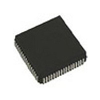
CY7C133-35JC Cypress Semiconductor Corp, CY7C133-35JC Datasheet - Page 5

CY7C133-35JC
Manufacturer Part Number
CY7C133-35JC
Description
Manufacturer
Cypress Semiconductor Corp
Datasheet
1.CY7C133-35JC.pdf
(13 pages)
Specifications of CY7C133-35JC
Density
32Kb
Access Time (max)
35ns
Sync/async
Asynchronous
Architecture
Not Required
Clock Freq (max)
Not RequiredMHz
Operating Supply Voltage (typ)
5V
Address Bus
11b
Package Type
PLCC
Operating Temp Range
0C to 70C
Number Of Ports
2
Supply Current
230mA
Operating Supply Voltage (min)
4.5V
Operating Supply Voltage (max)
5.5V
Operating Temperature Classification
Commercial
Mounting
Surface Mount
Pin Count
68
Word Size
16b
Number Of Words
2K
Lead Free Status / Rohs Status
Not Compliant
Available stocks
Company
Part Number
Manufacturer
Quantity
Price
Document #: 38-06036 Rev. *B
Maximum Ratings
(Above which the useful life may be impaired. For user guide-
lines, not tested.)
Storage Temperature ..................................... −65°C to +150°C
Ambient Temperature with
Power Applied.................................................. −55°C to +125°C
Supply Voltage to Ground Potential
(Pin 48 to Pin 24).................................................−0.5V to +7.0V
DC Voltage Applied to Outputs
in High-Z State .....................................................−0.5V to +7.0V
Electrical Characteristics
Electrical Characteristics
V
V
V
V
I
I
I
I
I
I
I
I
V
V
V
V
I
Notes:
Parameter
IX
OZ
OS
CC
SB1
SB2
SB3
SB4
IX
Parameter
5.
6.
7.
8.
OH
OL
IH
IL
OH
OL
IH
IL
BUSY pin only.
Duration of the short circuit should not exceed 30 seconds.
Tested initially and after any design or process changes that may affect these parameters.
At f=f
MAX
, address and data inputs are cycling at the maximum frequency of read cycle of 1/t
Output HIGH Voltage
Output LOW Voltage
Input HIGH Voltage
Input LOW Voltage
Input Leakage Current
Output Leakage Current
Output Short Circuit Current
V
Standby Current Both Ports, TTL
Inputs
Standby Current One Port, TTL
Inputs
Standby Current Both Ports,
CMOS Inputs
Standby Current One Port,
CMOS Inputs
Output HIGH Voltage
Output LOW Voltage
Input HIGH Voltage
Input LOW Voltage
Input Leakage Current GND < V
CC
Operating Supply Current
Description
Description
Over the Operating Range
Over the Operating Range (continued)
V
I
I
OL
OL
CC
[6, 7]
= 4.0 mA
= 16.0 mA
= Min., I
I
V
I
I
GND < V
GND < V
V
CE = V
Outputs Open, f = f
CE
CE
Outputs Open, f = f
Both Ports CE
0.2V, V
0.2V, f = 0
One Port CE
V
V
f = f
OL
OL
< V
Test Conditions
CC
CC
IN
IN
L
L
MAX
OH
= 4.0 mA
= 16.0 mA
< 0.2V, Active Port Outputs Open,
> V
CC
[5]
= Min., I
= Max., V
and CE
or CE
= –4.0 mA
[8]
IL
IN
CC
,
I
O
> V
< V
R
– 0.2V or
< V
R
> V
L
OH
CC
CC
[5]
or CE
OUT
> V
L
Test Conditions
CC
IH
and CE
= –4.0 mA
– 0.2V or V
, Output Disabled
IH
, Active Port
DC Input Voltage ................................................. −3.5V to +7.0V
Output Current into Outputs (LOW)............................. 20 mA
Static Discharge Voltage........................................... >2001V
(per MIL-STD-883, Method 3015)
Latch-up Current..................................................... >200 mA
Operating Range
Commercial
Industrial
= GND
MAX
MAX
, f = f
R
> V
[8]
[8]
Range
R
MAX
CC
> V
IN
– 0.2V,
[8]
CC
<
Min.
2.4
2.2
RC
−5
–
and using AC Test Waveforms input levels of GND to 3V.
7C133-35
7C143-35
Com’l
Ind.
Com’l
Ind.
Com’l
Ind.
Com’l
Ind.
Com’l
Ind.
Ambient Temperature
Typ.
−40
0
°
C to +70
Max.
°
0.4
0.5
0.8
+5
C to +85
Min.
2.4
2.2
−5
−5
Min.
2.4
2.2
−5
°
C
°
7C133-25
7C143-25
C
7C133-55
7C143-55
Typ.
170
170
100
100
40
40
90
90
3
3
Typ.
CY7C133
CY7C143
Max.
−200
5V ± 10%
5V ± 10%
250
290
140
160
120
140
Page 5 of 13
0.4
0.5
0.8
Max.
+5
+5
60
75
15
15
0.4
0.5
0.8
+5
V
CC
Unit
Unit
mA
mA
mA
mA
mA
mA
µA
µA
µA
V
V
V
V
V
V
V
V
[+] Feedback


