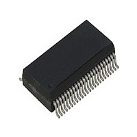
PI6C180VX Pericom Semiconductor, PI6C180VX Datasheet - Page 3

PI6C180VX
Manufacturer Part Number
PI6C180VX
Description
Manufacturer
Pericom Semiconductor
Datasheet
1.PI6C180VX.pdf
(7 pages)
Specifications of PI6C180VX
Number Of Outputs
18
Operating Supply Voltage (max)
3.465V
Operating Temp Range
0C to 70C
Propagation Delay Time
8ns
Operating Supply Voltage (min)
3.135V
Mounting
Surface Mount
Pin Count
48
Operating Supply Voltage (typ)
3.3V
Package Type
SSOP
Duty Cycle
55%
Operating Temperature Classification
Commercial
Lead Free Status / Rohs Status
Not Compliant
2-Wire I
The I
output and test mode enable.
The PI6C180 is a slave receiver device. It can not be read back.
Sub addressing is not supported. All preceding bytes must be sent
in order to change one of the control bytes.
Every bite put on the SDATA line must be 8-bits long (MSB first), fol-
lowed by an acknowledge bit generated by the receiving device.
During normal data transfers SDATA changes only when SCLOCK
is LOW. Exceptions: A HIGH to LOW transition on SDATA while
SCLOCK is HIGH indicates a “start” condition. A LOW to HIGH
transition on SDATAwhile SCLOCK is HIGH is a “stop” condition
and indicates the end of a data transfer cycle.
Byte1: SDRAM Active/Inactive Register
(1 = enable, 0 = disable)
Supply Current
Maximum Ratings
(Above which the useful life may be impaired. For user guidelines, not tested.)
I
I
I
DD
DD
DD
Storage Temperature........................................–65°C to +150°C
Ambient Temperature with Power Applied .........–0°C to +70°C
3.3V Supply Voltage to Ground Potential ..........–0.5V to +4.6V
DC Input Voltage ................................................–0.5V to +4.6V
Bit
7
6
5
4
3
2
1
0
2
Symbol
C interface permits individual enable/disable of each clock
2
C Control
Pin
45
44
41
40
36
35
32
31
SDRAM15 (Active/Inactive)
SDRAM14 (Active/Inactive)
SDRAM13 (Active/Inactive)
SDRAM12 (Active/Inactive)
SDRAM11 (Active/Inactive)
SDRAM10 (Active/Inactive)
SDRAM9 (Active/Inactive)
SDRAM8 (Active/Inactive)
Supply Current
(V
DD
= +3.465V, C
Parameter
Description
LOAD
= Max.)
BUF_IN = 0 MHz
BUF_IN = 66.66 MHz
BUF_IN = 100.00 MHz
Test Condidtion
3
Each data transfer is initiated with a start condition and ended with
a stop condition. The first byte after a start condition is always a
7-bit address byte followed by a read/write bit. (HIGH = read from
addressed device, LOW= write to addressed device). If the device’s
own address is detected, PI6C180 generates an acknowledge by
pulling SDATA line LOW during ninth clock pulse, then accepts
the following data bytes until another start or stop condition is
detected.
Following acknowledgement of the address byte (D2), two more
bytes must be sent:
1. “Command Code” byte, and
2. “Byte Count” byte.
Although the data bits on these two bytes are “don’t care,” they
must be sent and acknowledged.
Byte2: Optional Register for Possible Future Requirements
(1 = enable, 0 = disable)
Bit
Note:
Stresses greater than those listed under MAXIMUM RAT-
INGS may cause permanent damage to the device. This is a
stress rating only and functional operation of the device at
these or any other conditions above those indicated in the op-
erational sections of this specification is not implied. Exposure to
absolute maximum rating conditions for extended periods may affect
reliability.
7
6
5
4
3
2
1
0
Pin
28
21
SDRAM17 (Active/Inactive)
SDRAM16 (Active/Inactive)
(Reserved)
(Reserved)
(Reserved)
(Reserved)
(Reserved)
(Reserved)
Min.
Precision 1-18 Clock Buffer
Typ.
Description
Max.
230
360
2
PS8141F
PI6C180
Units
mA
12/13/04


