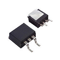
ISL9N306AS3ST Fairchild Semiconductor, ISL9N306AS3ST Datasheet

ISL9N306AS3ST
Specifications of ISL9N306AS3ST
Available stocks
Related parts for ISL9N306AS3ST
ISL9N306AS3ST Summary of contents
Page 1
... Thermal Resistance Junction to Case TO-220, TO-263 JC R Thermal Resistance Junction to Ambient TO-220, TO-263 JA R Thermal Resistance Junction to Ambient TO-263, 1in JA Package Marking and Ordering Information Device Marking Device N306AS ISL9N306AS3ST N306AP ISL9N306AP3 ©2002 Fairchild Semiconductor Corporation Features • Fast switching • 0.0052 DS(ON) • 0.0085 DS(ON) • ...
Page 2
... Fall Time f t Turn-Off Time OFF Unclamped Inductive Switching t Avalanche Time AV Drain-Source Diode Characteristics V Source to Drain Diode Voltage SD t Reverse Recovery Time rr Q Reverse Recovered Charge RR ©2002 Fairchild Semiconductor Corporation T = 25°C unless otherwise noted A Test Conditions I = 250 25V 20V GS ...
Page 3
... SINGLE PULSE 0. Figure 3. Normalized Maximum Transient Thermal Impedance 2000 1000 V = 10V 100 TRANSCONDUCTANCE MAY LIMIT CURRENT IN THIS REGION ©2002 Fairchild Semiconductor Corporation 150 175 125 Figure 2. Maximum Continuous Drain Current RECTANGULAR PULSE DURATION ( PULSE WIDTH (s) Figure 4. Peak Current Capability ...
Page 4
... GATE TO SOURCE VOLTAGE (V) GS Figure 7. Drain to Source On Resistance vs Gate Voltage and Drain Current 1.4 1.0 0.6 0.2 -80 - JUNCTION TEMPERATURE ( J Figure 9. Normalized Gate Threshold Voltage vs Junction Temperature ©2002 Fairchild Semiconductor Corporation (Continued) 150 T 100 - Figure 6. Saturation Characteristics 2 1.5 1.0 0.5 - Figure 8. Normalized Drain to Source On Resistance vs Junction Temperature 1 ...
Page 5
... R , GATE TO SOURCE RESISTANCE ( ) GS Figure 13. Switching Time vs Gate Resistance Test Circuits and Waveforms VARY t TO OBTAIN P R REQUIRED PEAK Figure 15. Unclamped Energy Test Circuit ©2002 Fairchild Semiconductor Corporation (Continued OSS Figure 12. Gate Charge Waveforms for Constant 500 400 t 300 f 200 ...
Page 6
... Test Circuits and Waveforms g(REF) Figure 17. Gate Charge Test Circuit Figure 19. Switching Time Test Circuit ©2002 Fairchild Semiconductor Corporation (Continued DUT g(REF) 0 Figure 18. Gate Charge Waveforms d(ON 90 DUT V GS 50% 10% 0 Figure 20. Switching Time Waveforms Q g(TOT g( g(TH OFF t d(OFF 10% 10% 90% 50% PULSE WIDTH Rev ...
Page 7
... JA times a coefficient added to a constant. The area, in square inches is the top copper area including the gate and source pads. 19.84 26.51 + ------------------------------------ - 0.262 + A rea ©2002 Fairchild Semiconductor Corporation , and the application’s ambient never exceeded (EQ ...
Page 8
... S2BMOD VSWITCH (RON = 1e-5 ROFF = 0.1 VON = 0.2 VOFF= -0.3) .ENDS NOTE: For further discussion of the PSPICE model, consult A New PSPICE Sub-Circuit for the Power MOSFET Featuring Global Temperature Options; IEEE Power Electronics Specialist Conference Records, 1991, written by William J. Hepp and C. Frank Wheatley. ©2002 Fairchild Semiconductor Corporation DPLCAP 5 10 RSLC1 ...
Page 9
... Fairchild Semiconductor Corporation DPLCAP 10 RSLC2 - 6 ESG 8 EVTHRES + ...
Page 10
... Fairchild Semiconductor Corporation JUNCTION th RTHERM1 CTHERM1 6 RTHERM2 CTHERM2 5 RTHERM3 CTHERM3 4 RTHERM4 CTHERM4 3 RTHERM5 ...
Page 11
... TRADEMARKS The following are registered and unregistered trademarks Fairchild Semiconductor owns or is authorized to use and is not intended exhaustive list of all such trademarks. ACEx™ FAST Bottomless™ FASTr™ FRFET™ CoolFET™ GlobalOptoisolator™ CROSSVOLT™ GTO™ DenseTrench™ ...


