IDT74FCT841ATSO IDT, Integrated Device Technology Inc, IDT74FCT841ATSO Datasheet

IDT74FCT841ATSO

Manufacturer Part Number
IDT74FCT841ATSO
Description
Manufacturer
IDT, Integrated Device Technology Inc
Type
D-Typer
Datasheet

Specifications of IDT74FCT841ATSO

Logic Family
FCT
Number Of Bits
10
Number Of Elements
1
Latch Mode
Transparent
Polarity
Non-Inverting
Technology
CMOS
Output Type
3-State
Package Type
SOIC
Propagation Delay Time
23ns
Operating Supply Voltage (typ)
5V
High Level Output Current
-15mA
Low Level Output Current
48mA
Operating Supply Voltage (min)
4.75V
Operating Supply Voltage (max)
5.25V
Operating Temp Range
-40C to 85C
Operating Temperature Classification
Industrial
Mounting
Surface Mount
Pin Count
24
Lead Free Status / Rohs Status
Not Compliant
© 2002 Integrated Device Technology, Inc.
FEATURES:
• A and C grades
• Low input and output leakage ≤ ≤ ≤ ≤ ≤ 1µA (max.)
• CMOS power levels
• True TTL input and output compatibility:
• High Drive outputs (-15mA I
• Meets or exceeds JEDEC standard 18 specifications
• Power off disable outputs permit "live insertion"
• Available in SOIC, SSOP, and QSOP packages
The IDT logo is a registered trademark of Integrated Device Technology, Inc.
INDUSTRIAL TEMPERATURE RANGE
FUNCTIONAL BLOCK DIAGRAM
IDT74FCT841AT/CT
FAST CMOS BUS INTERFACE LATCH
– V
– V
OH
OL
LE
OE
= 0.3V (typ.)
= 3.3V (typ.)
D
0
D
LE Q
Y
OH
0
D
1
, 48mA I
D
LE Q
OL
Y
1
)
FAST CMOS BUS
INTERFACE LATCH
D
2
D
LE
Q
Y
2
D
3
D
LE Q
1
Y
3
D
DESCRIPTION:
technology.
packages required to buffer existing latches and provide extra data width
for wider address/data paths or buses carrying parity. The FCT841T are
buffered, 10-bit wide versions of the popular FCT373T function. They are
ideal for use as an output port requiring high I
capacitive loads, while providing low-capacitance bus loading at both inputs
and outputs. All inputs have clamp diodes to ground and all outputs are
designed for low-capacitance bus loading in high-impedance state.
4
The FCT841T series is built using an advanced dual metal CMOS
The FCT841T bus interface latches are designed to eliminate the extra
All of the FCT841T high-performance interface family can drive large
D
LE Q
Y
4
D
5
D
LE Q
Y
5
D
INDUSTRIAL TEMPERATURE RANGE
8
D
LE Q
IDT74FCT841AT/CT
Y
8
D
OL
9
/I
D
LE
OH
.
Q
JUNE 2002
Y
9
DSC-2571/10

Related parts for IDT74FCT841ATSO

IDT74FCT841ATSO Summary of contents

Page 1

IDT74FCT841AT/CT FAST CMOS BUS INTERFACE LATCH FEATURES: • A and C grades • Low input and output leakage ≤ ≤ ≤ ≤ ≤ 1µA (max.) • CMOS power levels • True TTL input and output compatibility: – 3.3V ...

Page 2

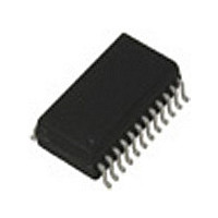
IDT74FCT841AT/CT FAST CMOS BUS INTERFACE LATCH PIN CONFIGURATION ...

Page 3

IDT74FCT841AT/CT FAST CMOS BUS INTERFACE LATCH DC ELECTRICAL CHARACTERISTICS OVER OPERATING RANGE Following Conditions Apply Unless Otherwise Specified: Industrial –40°C to +85° 5.0V ± Symbol Parameter V Input HIGH Level IH V Input LOW ...

Page 4

IDT74FCT841AT/CT FAST CMOS BUS INTERFACE LATCH POWER SUPPLY CHARACTERISTICS Symbol Parameter ΔI Quiescent Power Supply Current CC TTL Inputs HIGH I Dynamic Power Supply CCD (4) Current (6) I Total Power Supply Current C NOTES: 1. For conditions shown as ...

Page 5

IDT74FCT841AT/CT FAST CMOS BUS INTERFACE LATCH SWITCHING CHARACTERISTICS OVER OPERATING RANGE Symbol Parameter t Propagation Delay PLH (LE = HIGH) PHL t Propagation Delay PLH PHL t Output Enable Time, PZH OE ...

Page 6

IDT74FCT841AT/CT FAST CMOS BUS INTERFACE LATCH TEST CIRCUITS AND WAVEFORMS OUT V IN Pulse D.U.T Generator . R T Test Circuits for All Outputs DATA INPUT t SU TIMING INPUT ASYNCHRONOUS CONTROL PRESET CLEAR ETC. SYNCHRONOUS CONTROL ...

Page 7

IDT74FCT841AT/CT FAST CMOS BUS INTERFACE LATCH ORDERING INFORMATION IDT XX FCT XXXX Temp. Range Device Type CORPORATE HEADQUARTERS 6024 Silver Creek Valley Road San Jose, CA 95138 X Package 841AT 841CT 74 for SALES: 800-345-7015 or 408-284-8200 ...

Related keywords