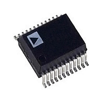
AD7011ARS Analog Devices Inc, AD7011ARS Datasheet - Page 2

AD7011ARS
Manufacturer Part Number
AD7011ARS
Description
Manufacturer
Analog Devices Inc
Datasheet
1.AD7011ARS.pdf
(12 pages)
Specifications of AD7011ARS
Device Type
Modulator
Modulation Type
Quadrature
Pin Count
24
Package Type
SSOP
Lead Free Status / Rohs Status
Not Compliant
Available stocks
Company
Part Number
Manufacturer
Quantity
Price
Part Number:
AD7011ARS
Manufacturer:
ADI/亚德诺
Quantity:
20 000
Part Number:
AD7011ARSZ
Manufacturer:
ADI/亚德诺
Quantity:
20 000
f
AD7011–SPECIFICATIONS
Parameter
DIGITAL MODE TRANSMIT SPECIFICATIONS
ANALOG MODE SPECIFICATIONS
REFERENCE & CHANNEL SPECIFICATIONS
LOGIC INPUTS
LOGIC OUTPUTS
POWER SUPPLIES
NOTES
1
2
3
4
5
Specifications subject to change without notice.
MCLK
Operating temperature ranges as follows: A Version: –40 C to +85 C.
See terminology.
Measured in continuous transmission and Burst Mode with the I and Q channels ramping up and down at the beginning and end of a burst.
Headroom must be allowed for the transmit DACs such that offsets in I & Q transmit channels can be calibrated out. Therefore, the full range of the I and Q DACs
are not available to the user. The user should ensure that binary codes greater than or less than the maximum or minimum are not loaded into the I or Q DACs.
Measured while the digital inputs to the transmit interface are static and equal to 0 V or V
Number of Channels
Output Signal Range
Differential Output Range
Signal Vector Magnitude
Error Vector Magnitude
Offset Vector Magnitude
IS-54 Spurious Power
No. of Channels
Resolution
Output Signal Range
Differential Output Range
DAC Update Rate
SNR
Differential Offset Error
Group Delay Matching Between I & Q Outputs
Coding
Maximum and Minimum DAC Codes
Reference, V
Reference Accuracy
I and Q Gain Matching
Power-Down Option
V
V
I
C
V
V
V
I
INH
DD
INH
INL
OH
OL
DD
= 3.1104 MHz; Analog Mode, f
IN
@ 30 kHz
@ 60 kHz
@ 90 kHz, 120 kHz
Transmit Section Active
Transmit Section Powered Down
, Input Capacitance
, Input Current
, Input Low Voltage
Output Low Voltage
, Input High Voltage
Output High Voltage
REF
2, 3
2
2
2
MCLK
= 2.56 MHz, POWER = V
5
4
1
(V
AA
= V
DD
AD7011ARS
2
V
+V
0.875
1
2.5
0.5
2.5
–35
–30
–70
–65
–75
–70
2
10
V
160
60
55
30
Twos Complement
+450/–450
2.46
Yes
V
0.9
10
10
V
0.4
4.5/5.5
8
6
35
5
REF
REF
2V
15
5
0.2
DD
DD
. All specifications are T
DD
REF
= +5 V
REF
– 0.9
– 0.4
+ V
/2
–2–
V
/3
7.5%
REF
REF
/4
/3
10%; Test = AGND = DGND = 0 V; Digital Mode,
DD
.
V min/V max
Units
Volts
Volts
Volts max
% rms typ
% rms max
% typ
% max
dB typ
dB max
dB typ
dB max
dB typ
dB max
Bits
Volts
Volts
kHz
dB typ
dB min
mV max
ns typ
max/min
Volts
%
dB max
V min
V max
FA max
pF max
V min
V max
mA max
mA typ
A max
A max
MIN
to T
MAX
unless otherwise noted.)
Test Conditions/Comments
(ITx – ITx) and (QTx – QTx)
For Each Analog Output
I Channel = (ITx – ITx) and
Q Channel = (QTx – QTx)
Measured Differentially
(ITx – ITx) and (QTx – QTx)
For Each Analog Output
I Channel = (ITx – ITx) and
Q Channel = (QTx – QTx)
MCLK/16; f
Generating a 10 kHz Sine Wave
Post Calibration
Measured @ 10 kHz
Power = 0 V
|I
POWER = V
MCLK Active
MCLK Inactive
|I
OUT
OUT
|
|
40 A
1.6 mA
MCLK
DD
= 2.56 MHz
REV. B


